| Issue |
Eur. Phys. J. Appl. Phys.
Volume 97, 2022
Special lssue on ‘EELS - Review over the last 50 years by Christian Colliex’
|
|
|---|---|---|
| Article Number | 38 | |
| Number of page(s) | 47 | |
| Section | Imaging, Microscopy and Spectroscopy | |
| DOI | https://doi.org/10.1051/epjap/2022220012 | |
| Published online | 24 June 2022 | |
https://doi.org/10.1051/epjap/2022220012
Review Article
From early to present and future achievements of EELS in the TEM
Laboratoire de Physique des Solides (UMR CNRS 8502), Bât. 510, Université Paris-Sud, Université Paris Saclay, 91400 Orsay, France
* e-mail: This email address is being protected from spambots. You need JavaScript enabled to view it.
Received:
18
January
2022
Received in final form:
23
February
2022
Accepted:
24
February
2022
Published online: 24 June 2022
Abstract
This paper reviews the implementation of Electron Energy Loss Spectroscopy (EELS) in a Transmission Electron Microscope (TEM), as an essential tool for advanced analytical studies, exhibiting a unique level of performance in terms of spatial resolution down to the interatomic distances for imaging and sensitivity down to the single atom for elemental identification. In terms of spectral resolution, it offers access with a resolution as good as a few meV, to a very broad spectral domain extending from tens of meV (in the IR) up to a few keV (in the X-ray). This new generation of instrument (EELS+(S)TEM) is now routinely used to investigate the structural, spectral, electronic and chemical properties of a wide range of materials and to broaden spectacularly the field of novel information which it provides. A first part of the paper describes the major progress in advanced instrumentation brought by the novel pieces of equipment (spectrometers, monochromators, aberration correctors and detectors) together with the newly elaborated tools for the acquisition and processing of huge data collections. The second part is devoted to the description of the information contained in a global EELS spectrum: (i) from the core-loss domain implying excitations from inner-shell atomic electrons and its application in elemental, chemical and electronic mapping; (ii) from the low-energy domain exhibiting individual or collective excitations of the valence and conduction electron gas, with its most recent developments in band gap mapping and nanoplasmonics; (iii) in the ultra-low energy domain, which is now in its infancy, the surface collective electron excitations, molecular bonds and the vibrations of phonons at surfaces and in the bulk of nanostructures. The third part is devoted to the exploration of unconventional domains of applications, which in many cases associate the EELS acquisition with the generation and the capture of other signals in various environments, in situ operation (temperature, pressure...), absorption or generation of photons (cathodoluminescence, X-ray emission), acquisition and handling of multidimension data (space, energy, momentum, time). In conclusion, EELS fifty years after its first recognition as a useful actor in the development and promotion of the analytical microscopy, has nowadays become an essential tool for the acquisition of many physical parameters with ultimate resolution, thus opening new routes in nanophysics to be explored.
© C. Colliex, Published by EDP Sciences, 2022
 This is an Open Access article distributed under the terms of the Creative Commons Attribution License (https://creativecommons.org/licenses/by/4.0), which permits unrestricted use, distribution, and reproduction in any medium, provided the original work is properly cited.
1 Introduction
Electron Energy Loss Spectroscopy (EELS) has established itself for decades as a powerful method for the investigation of excitations of the electron population in a solid material. Furthermore, when attached to the column of a transmission electron microscope (TEM), it has become nowadays an undisputable analytical component on all recently acquired instruments. The first measurements of the energy of electrons transmitted through thin foils were reported in the forties by Hillier and Baker [1] and by Ruthemann [2] suggesting that the detected signals, in particular, the K-edges in carbon, nitrogen and oxygen, could be used as a micro-analytical tool. However it took two decades to see substantial progress in this domain. Boersch and colleagues at Berlin developed in the sixties a dedicated high resolution energy-loss measurement bench combining a monochromator and an analyser achieving a 50 meV resolution on EELS spectra of argon gas [3]. On its side, the Orsay group designed a mirror-prism device, known as the Castaing-Henry one [4], and introduced it into the column of a TEM for both analysing and filtering the energy of the electrons contributing to the formation of an image. A few years later, relying on these instrumental developments, several groups undertook more systematic studies on the use of core-loss signals for spatially resolved elemental analysis. The Cambridge group [5] used a simple magnetic spectrometer fixed under the bottom of a Conventional TEM [6], similarly for the Chicago group but under a dedicated Scanning TEM [7–9]. As for the Orsay group, it undertook a systematic study of some major characteristic edges detected between typically a few tens and a few hundreds of eV [10–12]. The following decade, the seventies, was rich in studies, with the contribution of Egerton to establish the basics of quantitative elemental analysis from the recorded core-loss spectra [13,14] and by the seminal papers by Isaacson and Johnson [15] and by Colliex et al. [16] defining the frame in which EELS should develop into a general and powerful analytical tool. A couple of years later, at the end of the seventies, two workshops on analytical electron microscopy were organized at Cornell U., in 1976 (see [17] for a report) and in 1978, The outcome of these very lively schools definitely established EELS (electron energy loss spectrometry) as one of the two major tools, together with EDX (energy dispersive X-ray spectrometry), giving access to qualitative and quantitative measurements of the elemental distribution mapping, and chemical state analyses in the micro-size observation areas. In the following years, EELS established itself as an undisputed complementary technique in the (S)TEM to access a new level of information besides imaging and diffraction. This observation led me to write a review entitled “Electron energy loss spectroscopy in the electron microscope”, which was published in 1984 in the Advances in Optical and Electron Microscopy [18]. However, as this manuscript has not been digitized and is therefore off most citation libraries, it has not received much consideration. Very recently, Elsevier has come across this failure and has decided to reprint it as it was originally, in the series Advances in Imaging and Electron Physics, volume 211 (2019), which means 35 five years after its first publication [18] !!
It is then obvious that, over such a time, instrumentation and theory have spectacularly progressed and that in terms of performance and fields of applications, EELS in the (S)TEM has little in common with that depicted in 1984. As an illustrative example of the jumps in accessible ranges of spectral excitation, Figure 1 compares EELS spectra displaying plasmon peaks, i.e. collective excitations of the valence and conduction electrons of the investigated material, recorded in the seventies and nowadays.
In the “old” spectrum (left) extracted from the review paper in 1984, the whole energy scale covers 100 eV and displays lines distant of about 16 eV attributed to the excitation of 1 to 6 bulk plasmons by the incident 100 keV electrons of the microscope going through a foil of silicon, typically a few hundreds of nm thick. As for the “new” spectrum (right), the whole energy range covers 1 eV, and it displays variable numbers of surface plasmons of energy ranging from 5 to 500 meV, depending on the length of the excited copper nanorod. In terms of investigated optical domains, it corresponds to a jump from a typical far-UV to a typical far-IR range. The scope of the present text is therefore to offer, through a few glimpses at subjectively selected recent achievements, a significantly updated view of the present state and impact of EELS in the new generation of (S)TEM. After a survey of the major breakthroughs, as well instrumental, methodological as theoretical, realized over the past decades, this paper will describe the three major types of available information and their field of use, following the covered energy range of the measured energy loss: core-loss above 50 eV up to a few thousands, individual and collective excitations of the electron gas from 1 to 50 eV, ultra-low energy electron excitations and phonons below typically 1 eV.
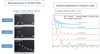 |
Fig. 1 EELS spectra displaying on the left the excitation of bulk plasmons in Si as recorded in the seventies (published in Colliex [17a]) and on the right the excitation of surface plasmons on long Cu nanorods as recorded very recently with a STEM of the latest generation (courtesy A. Gloter and X. Li, private communication, 2019). |
2 Major breakthroughs
2.1 Advanced instrumentation
In the context of a TEM column, the EELS technique is associated to a new dimension as it provides a spatially resolved spectroscopic information. Practically, one measures for a primary intensity I0 of electrons traveling with energy E0, the intensity of the beam transmitted through the specimen at position r(x,y), scattered within a solid angle δΩ around the direction θ and having suffered an energy loss in a spectral window δE around the energy loss ΔE, i.e. an intensity I(r,θ, ΔE). Generally, the angular acceptance is defined by an aperture of semi-angle β and there are two major approaches (scanning or fixed beam) to access the spatially resolved EELS information. They are the energy analysis mode delivering spatially resolved spectra Ir (ΔE) and the energy filtering one delivering energy filtered images IΔE (r), respectively acquired with a STEM or a CTEM microscope. Let us now focus on the analysis mode (STEM-EELS), the scanning one.
2.1.1 The STEM microscope with parallel EELS
In the scanning mode, an EELS spectrum is acquired for each position (x,y) of the probe on the surface of the thin foil, with a spectrometer working as an analyzer. The spatial resolution is then defined by the probe size, as long as the local thickness does not give rise to a noticeable probe broadening across the specimen. The basic architecture of such a STEM is made of an electron source, of a focused illumination on the specimen, and of a set of detector channels collecting the electrons scattered in different solid angles, one of them including the velocity analyzer producing the EELS signal (see Fig. 2 left). All these components have regularly become technologically more advanced in terms of design and stability and new electron optical devices have been introduced. Basically, the best level of performance accessible today, i.e. typically 0.1 nm in spatial resolution and 10 meV in energy resolution, requires: (i) a high brightness electron gun associated with a monochromator; (ii) an aberration-corrected focusing optics delivering the smallest probe on the specimen (iii) an optimized transfer electron optics between the specimen exit surface and the different collector apertures; (iv) an aberration-corrected energy-loss spectrometer achieving optimized energy resolution and (v) an electron detector of optimum efficiency and dynamic range. These components are all combined in the design of the latest generation of microscopes aiming at optimum performance for EELS studies, such as shown in Figure 2, right.
The high-brightness electron source, with B = dI/(dS.dΩ) in A/cm2 sr, is essential for delivering the highest signal/noise (SNR) in all recorded signals. It is generally of cold field-emission type (as well in the VG as in the NION microscope) producing an electron beam with a 0.25 eV natural width, the slit within the energy dispersing monochromator being capable to reduce it to below 10 meV [19]. The primary voltage can be fixed at different values from typically 30 to 200 kV. If higher voltages deliver higher brightness beams and improved spatial resolution, the lower ones are preferably chosen to study very thin layers (a few atomic layers thick such as 2D materials) where they deliver more intense scattering signals, are less damaging for beam sensitive materials and can also display sub-atomic spatial resolution with the support of aberration-corrected focusing lenses.
The VG microscopes which have followed in the 70–80s the original Crewe's design [9,21] and its first imaging of individual heavy atoms deposited on thin carbon layers [22] have demonstrated their capacity in delivering on the specimen surface, currents of a few hundred pA in a probe of 0.25 to 0.50 nm, which has evidently been quite instrumental in the success of analytical electron microscopy. With the combination of structural images through the angular dark field detector and of EELS signals on characteristic core-loss, the accessible SNR was demonstrated to be sufficient for the identification of individual atoms [23]. With the introduction of aberration correctors following the designs of Haider [24] or Krivanek [25], an explosion of elemental and electronic mapping with atomic resolution occurred [26–28], made possible by an attainable spatial resolution of 50 pm at 200 kV and a current up to 1 nA in a probe of 150 pm.
In the post-specimen part of the STEM, a multi-detector configuration collects the whole, or an angularly discriminated fraction of the transmitted electrons. In the first case, the micro-diffraction pattern is then available for each position of the probe on the specimen, and can thus give access to coherent diffractive imaging generally known as ptychography. On the other hand, the selection of the beams collected by a set of circular apertures of different inner and outer diameters delivers the standard Bright Field (BF), Annular Bright Field (ABF), High Angle or Medium Angle Annular Dark Field (HAADF or MAADF) images which all carry information on the local structure and composition of the specimen.
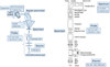 |
Fig. 2 Major components of the two STEM columns dedicated to EELS studies presently in operation in Orsay : (left) the VG HB501 received in 1980, (right) the NION Chromatem received in 2018. With respect to the simple VG microscope, the NION one incorporates three new major electron optical components: a monochromator, an aberration corrector in the probe forming optics, an aberration-corrected EELS spectrometer and associated parallel EELS detector, the schematic cross section of the monochromated NION column is extracted from [20]. Associated with these figures are characteristics of key parameters of the probe (intensity, lateral size, energy width) for the two instruments. |
2.1.2 Spectrometers, filters and monochromators [29,30]
One of these apertures, of limited angular acceptance, is followed by the velocity analyzer of the transmitted electrons. This spectrometer is nowadays most generally of the homogeneous magnetic field type which bends the analyzed beam by an angle of 90° with a discriminating power, or dispersion, of the different velocities in its image plane, expressed in μm/eV. Practically, the energy resolution of this spectrometer is related to the smallest size of the spot in its dispersion plane, which is practically a sum of different contributions, two of the dominant ones being the aberrations accompanying the imperfect focusing of the magnet and the other one accompanying the natural energy width δE0 of the incident electrons on the specimen. Consequently, continuous effort has been devoted to remedy these limitations, concerning the design of the spectrometer itself and the transfer optics between the specimen exit surface and the entrance face of the magnet. Nowadays, the most popular EELS analyzer, and filter, made commercially available by Gatan US, can be fitted to nearly any type of (S)TEM, to any primary energy between 30 and 300 kV, and offers energy resolutions mostly controlled by δE0 = 0.25 eV for a cold FEG. The spectacular advances bringing the attainable energy resolution in the range of 10 meV, have been the introduction of monochromators at the exit of the electron source. They are made of another energy dispersing system and of a selecting slit. Different types have been built and have now been made commercially available. They are of electrostatic or magnetic type or combining both of them [29,30]. In the column shown in Figure 2b, an alpha-shaped magnetic monochromator has been installed, it is basically made of two parallel electron energy loss spectrometers back to back with a selecting slit in the median plane of the whole system. It therefore selects only a fraction of the spectrum to be used in the rest of the column. Most recent measurements on the Orsay NION Chromatem microscope have demonstrated a FWHM width of 5 meV (Fig. 3).
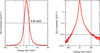 |
Fig. 3 Demonstration of the high energy resolution offered by the latest generation of monochromatized STEM (NION Chromatem) : (left) zero loss peak (ZLP) recorded in vacuum exhibiting a symmetric profile of FWHM below 5 meV; (right) same peak displayed on a logarithmic scale, demonstrating a large reduction of intensity in its tail of the order of 10−3 over an energy window of 40 meV, thus giving access to the recording of very low-energy excitations. |
2.1.3 Detectors
The final important component in the chain of performing EELS in a STEM is the detector which measures the flux of electrons in the dispersion plane of the spectrometer and transfers it through a convenient converter to the digital acquisition and processing unit. In the early stages of EELS acquisition, the EELS spectra such as those displayed in [18], one of them being shown in Figure 1a, were acquired on photographic plates and digitized with a microdensitometer device. They constituted a first generation of parallel acquisition. Then, over a typical period of 15 years, the spectra were acquired sequentially by ramping the inelastic electron distribution in front of a detection slit followed by a plastic scintillator and photomultiplier or by a first generation of semi-conductor detector. This was the situation described in [18], in which the access to parallel recording of energy-loss spectra was only briefly mentioned “as an important potential improvement in EELS spectroscopy” and that “an important major step forward should be awaited during the next two years”. This was written in 1984, and actually it has benefitted of perpetual developments and progress since then.
Very rapidly indeed, following preliminary exploration by Shuman [31], the huge potential of the parallel acquisition of all energy loss channels through an array of diodes was confirmed [32,33] and it then became an undisputed component in any commercially EELS system for the next decades. In particular, it has been a key for the success of all hyperspectral (or spectrum-image) techniques developed in the nineties, see further on. Charge Coupled Devices (CCD) cameras became the most widely used detectors over the past decades. As a matter of fact, they are made of three components (see Fig. 4 top): in these indirect cameras, the incident high energy electron is first transformed into a bunch of photons in a scintillator. The emitted photons are then transferred via an optical imaging lens or a bunch of optical fibers, onto the array of semiconducting cells, typically 15–20 μm in size, of the CCD chip where they are converted into electron-hole pairs separated by a biasing voltage. The charge in an individual cell increases nearly proportional to the number of impacting electrons. During the read-out, this charge is transferred into an analogue-to-digital conversion chip for further storage and processing.
Over the years, technological developments have regularly promoted these indirect detectors to a high level of performance in terms of point spread function, dynamic range, speed of acquisition. For instance, in order to accept the large dynamic range encountered in EELS, Dual EELS, introduced simultaneously in Glasgow and in Orsay [34,35] and made commercially available by Gatan, consists in rapidly switching both in energy and laterally the EELS spectrum on different parts of the detector. Another approach uses two different register schemes (Low Noise CCD or Electron Multiplying CCD) for the acquisition of very low counting and very fast spectro-microscopy. This combination has opened a path to the fast acquisition of EELS spectra, such as demonstrated in Figure 5. The identification of heavy atoms (Tb and Th) in rapid motion on a thin carbon layer, has been made possible using a home-made ultra-fast parallel EELS detection system run in the EM-CCD mode in an aberration-corrected NION microscope [36]. The characteristic Th O45 and Tb N45 edges, respectively at 88 eV and 146 eV, are clearly seen in individual spectra recorded in 100 μs.
In spite of these advances, some of the intrinsic drawbacks of the indirect camera relying on an electron-photon conversion, such as its associated relatively large point spread function and limited detection quantum efficiency (DQE), have stimulated research on the design, realization and use of direct electron detection and counting units. Over the last decade, radiation-hard direct detection systems employing a patterned CMOS (complementary metal oxide semiconductor) architecture (see Fig. 4 bottom), have demonstrated their ability to be used, as well in conventional low dose electron microscopy [37], as more recently in EELS [38]. In the first case, a monolithic active pixel sensor (MAPS) technology is used to fabricate uniform large format (>1 Mégapixels) sensors of small lateral size (typically 5–10 μm) in a thin Si membrane (around 25 μm), through which high energy electrons are transmitted with very weak lateral spread. These detectors have demonstrated for incident electrons of 300 kV very high DQE and therefore their capability to detect and count individual electrons. Consequently, this new generation of imaging device has revolutionized the field of cryo-electron microscopy in structural biology [39]. As for the detection of EELS spectra generated by incident electrons typically of 60 to 200 kV, these MAPS detectors suffer from scattering of the signal across several pixels. Consequently, an alternative technology developed for particle physics is presently being tested. This Medipix3 hybrid pixel sensor incorporates advanced analogue processing and digital conversion circuitry at the individual pixel level [40].
In these devices see Figure 6a, impinging electrons enter a 300 μm to 500 μm thick silicon layer. The created electron-hole pairs are separated and the charges are read through a net of pads at the bottom. Each net has its own analog and digital circuitry giving the capability to detect each primary electron and count them into the cell at a rate above 1M e- per second. These detectors no longer require a blanking of the beam during image readout. Rates higher than 100 000 spectra per second are already achieved. Ultimately using Timepix3, Timepix4 in the near future, each electron can be tagged with time, and read immediately. “Fast spim” mode using scan speed as fast as 100 ns per pixel has been achieved (to be published by Y. Auad et al. (2021)). With these readout rates, a single spectrum image is acquired within seconds and added while specimen drift is measured and canceled online.
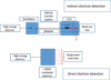 |
Fig. 4 The two different schemes of parallel detection of EELS in operation : the indirect one with electron-photon-electron CCD conversion (top) and the direct detection CMOS camera (bottom). |
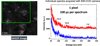 |
Fig. 5 Fast parallel EELS spectroscopy on individual atoms or clusters made of a few atoms in rapid motion on a thin carbon foil : (left) HAADF image of the analyzed area, (right) a selection of two spectra recorded at the apex of the white spots at the end of the blue and red arrows in (a). These individual spectra are extracted from a collection of 217 × 230 spectra in a spectrum-image recorded at the rate of 100 ms/spectrum, 0.35 Å/pixel (see [36]). |
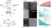 |
Fig. 6 On left, images (a and b) represent a schematic of Medipix3 pixel architecture. In a) the primary electron enters a few hundred microns silicon layer. Electron hole pairs are created. Either electron or hole drift towards the contact at the bottom, upon bias polarity. In b) an analog front end transform the current into a voltage. When it reaches the threshold, a digital counter is incremented. At the end of exposure time, this counter transferred to a computer. On right 6c) a typical experiment on DyScO3/SrRuO3 interface using a Nion UltraSTEM 100 kV 30 mrad probe with 10 pA is displayed. Left images show a sum of 101 scans on the area while drift is measured and canceled online. No post processing is done. Top right image is the actual drift during whole exposure. Middle right image is a single spectrum on a single scan on a pixel. Dwell time per pixel is 200 μs, pixel size is 40 × 40 pm and total experiment time is 8 minutes. The sum averages all scan noises. The Dy-Dy zig-zag chain of 70 pm is clearly visible in HAADF and Dy map (courtesy Marcel Tencé and Alexandre Gloter). |
2.2 Acquisition and processing of multidimensional spectrum-imaging data
In the previous paragraph, we have described in detail how the scanning illumination combined with a parallel acquisition spectrometer now delivers high numbers of spectra when scanning the incident probe of a STEM microscope on a region of interest of the sample. Similarly, as mentioned earlier, an alternative approach to record high numbers of spatially resolved spectra is the fixed beam illumination CTEM microscope equipped with an energy filtering device (Energy Filtering Transmission Electron Microscopy (EFTEM)). In this case, an energy filter derived from the early Castaing and Henry filter [41] or of an all-magnetic type, is inserted in the column of a TEM. Alternatively, an upgraded combination of a magnetic sector followed by an electron optical transfer system at the bottom of the column also delivers energy-filtered images made of only the electrons transferred through a slit, the width of which determines the selected energy window.
Whatever the approach (STEM-EELS or EFTEM), multidimensional spectrum-images or image spectra data (SPIM) in a mixed space (spatial made of N × N pixels and spectral made of n channels) are nowadays acquired in huge quantities. As introduced by Jeanguillaume and Colliex [42], these 3D data cubes can be built as a collection of parallel EELS spectra or as a stack of energy filtered images, see Figure 7. These modes have been practically implemented in the early nineties [43,44]. Since then it has been confirmed that the STEM-EELS approach is best adapted for the recording of spectrum-images made of a large numbers of energy loss channels while the EFTEM is more adapted to the recording o few energy filtered images (at best with n = 1) images with great values of N. Furthermore, in terms of total incident dose, the parallel EELS detection mode of a scanned incident probe is by far less damaging that the n times illumination of the whole area for the acquisition of the equivalent spectral information per pixel.
Nowadays, with a well-equipped STEM-EELS instrument, series of 3D spectrum-images of typical size 200 × 200 pixels and over 1000 energy channels are easily recorded, producing huge data sets of the order of 10 GB, which require well adapted tools, as well in hardware as in software, to extract the best information out of them. The present trend is also to increase the data set dimension from 3D to 4D, with time-resolved SPIMs, or higher when recording spectra under different tilt angles for accessing to the z-axis. Consequently, new processing schemes have been developed to go beyond the standard tools which have been elaborated over decades to process individual spectra.
Denoising: One limitation of the spectrum-image (SI) made of many pixels is the short dwell time for the acquisition of the spectrum on a given pixel which is necessary limited to a few ms to maintain the total recording time at a reasonable value not suffering from significant electronic instabilities or specimen shifts and radiation damage. Consequently, the available signal in an EELS channel is generally weak and the huge potential of the approach may be compromised by a low signal/noise ratio. Denoising of the data therefore represents a most important challenge.
Usually SIs are denoised using principal component analysis (PCA). PCA is a statistical method based on the fact that neighbouring energy channels are highly correlated and convey redundant information about the pixels. Thus PCA uses an orthogonal transformation to describe the data with new axes (i.e. new ‘abstract’ spectra). These new axes are designed as components. By selecting only a limited number of axes (or components) we obtain a dimensionality reduction. If we reconstruct the data using only these components we extract the important information and eliminate the components representing noise. PCA is available in most data processing toolboxes (Matlab, Scikit, Hyperspy [45]…) and has been applied to denoise SI datasets with success due to its simplicity of use.
However, it has some limitations. As the data are non-completely linear, relevant information may be retained in the low variance components, consequently be lost and lead to artefacts as shown in [46]. The number of retained components must be chosen with great care and constitutes a sensible parameter of this denoising technique. Moreover, owing to the orthogonality constraint, the components found by the decomposition process cannot be identified with the real components of the system, that is the spectra of the different elements of the probed sample. Another limitation is that each individual spectrum is processed independently of spatial positions and the spatial correlations between pixels are not taken into account for denoising. Some authors have tried to take into account the 3D character of the SI by using tensor decomposition [47]. These methods are far more computationally expensive than PCA and are not widely used at the present moment.
Unmixing: In order to get a more quantitative analysis consisting in a set of components corresponding to the real spectra of the chemical constituents of the sample, and their relative abundances, other approaches have to be employed.
First attempts used Independent Component Analysis (ICA) with some success [48,49]. ICA has been implemented on Hyperspy Toolbox. However, ICA is based on the assumption of mutually independent sources, which is a strong mathematical condition that might be not fulfilled in the case of SIs since the sum of abundances of the different components is constant. Nevertheless, this approach may give satisfactory results in some cases but its limitations may have restricted its use since spectral unmixing is not still widely applied in EELS community.
Other unmixing approaches developed for remote sensing data, and exploiting geometrical features of hyperspectral mixtures (Vertex Component Analysis[50]), or Bayesian statistics (Blind Linear Unmixing [51]) have been applied to SIs [52].
Inpainting: In order to reduce electron dose effects and to increase the acquisition speed of SIs, a random scan acquisition mode has been proposed and put into operation at LPS Orsay [53]. This inpainting technique uses a table containing a list of pixels defining the path of the scan. Instead of scanning sequentially, line per line, the region of interest, the pixels are probed in a pre-defined pattern, usually in a random sequence. The whole SI is acquired and can be processed as an usual one, but it is also possible to extract subsampled random sparse images. Specific reconstructions approaches have been developed, which exploit the spectral redundancy and the spatial properties of the SI [54]. It is then possible to retrieve a complete SI from a partial sequence of pixels. In Figure 8, the potential of this technique is illustrated for the reconstruction of elemental maps at atomic resolution from a random selection of individual spectra. This random scan mode has recently been applied with great success in different spectro-microscopies techniques, as well in atomically spatially resolved EELS elemental mapping as in nanoscale CL [55].
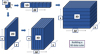 |
Fig. 7 Building a 3D data cube either as collection of parallel EELS spectra recorded at different points (x,y) on the specimen in a STEM microscope or as a stack of energy filtered images with energy ΔE (from [42]). The individual bit of useful information (0D) is the intensity recorded in an energy-loss channel of width δE at ΔE and on a pixel size of area δx x δy at (x,y). |
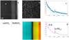 |
Fig. 8 Demonstration of the output of random scan acquisition and inpainting reconstruction for atomically resolved EELS elemental mapping: (a) HAADF Image of the region of interest (189 × 200 pixels in the red bordered square) at the interface between two oxide crystals LaAlO3/NdNiO3; (b) definition of the randomly selected 20% pixels over the region of interest; (c) example of an individually acquired EELS spectrum on the LaAlO3 area, exhibiting two characteristic edges O-K and La-M45, acquisition time is 10 ms so that the spectrum is rather noisy; (d) elemental maps, represented in an arbitrary color scheme (La (cyan)-Ni (green)-Nd (red)), obtained after inpainting of the randomly selected 20% spectra; (e) individual spectrum obtained after inpainting for a non-directly acquired spectrum (courtesy of Nathalie Brun). |
3 Delivered information in an EELS spectrum and fields of use
An electron energy-loss spectrum reflects the response of the charged population (electrons and ions) of the solid material under investigation, practically a thin layer of thickness ranging from an atomically thick monolayer to a section up to a few hundred angströms, to the external disturbance created by the electric field accompanying the high energy incident electron travelling through or in the close neighbourhood of the external surface of the specimen. Figure 9 shows the different contributions in this EELS response for a thin MgO layer. It covers significant scales on both the energy axis, from 70 meV up to 1500 eV, and on the intensity one, over a factor of 106 typically. Such a spectrum is recorded through an aperture after the specimen which collects all electrons scattered within a solid angle dΩ of semi-angle α around their incident trajectory.
The response of the electron population of the solid appears in the two major energy ranges:
In blue, from typically 50 eV to highest values (a few thousand eV), i.e. in the far UV up to the X-ray spectral domain, the core energy-loss domain. It corresponds to the excitation of the atomic core–shell electrons, in the present case of the 1s electrons of oxygen atoms (O-K edge) and of Mg atoms (Mg-K edge) respectively at 532 eV (see insert O-K) and 1305 eV. They appear as more or less abrupt edges followed by some extended oscillating profile, superposed of a continuously decaying background. The Mg-L23 edge (around 50 eV) lies at the upper limit of the low-energy loss domain but it is in fact of core-loss type.
In green, from about 1 up to 50 eV, i.e. over the near IR-visible-near UV spectral domain, the low energy-loss domain. It involves all excitations of the rather delocalized electrons from the conduction, the valence and the moderately bound electrons. It exhibits the dominant excitations of the EELS spectra, in particular the collective excitations, plasmons culminating at 22.5 eV in the case of MgO and a substantial amount of individual interband transitions (see insert “band gaps”).
In the well-established scheme of electronic levels in a solid, these excitations can be represented either as individual transitions between occupied and unoccupied electron states, or as collective excitations of the rather-free electron gas (see Fig. 10).
As for the zero-loss peak (in red), it corresponds to all electrons which have not lost any measurable energy-loss. As a matter of fact, with the advent of monochromated high energy electron beams such as those displayed in Figure 3, it is now possible to visualize and measure on the high energy tail of the ZLP, weak signals in the range of 50 to 500 meV (i.e. well in the IR spectral photonic range) corresponding to the excitation of phonons, which constitutes one major progress over the past recent years [19].
In the review paper published in 1984 and in 2019 [18], the basic physics involved in the core and low-energy loss domains has been extensively described. Therefore, in the following paragraphs, we will focus on the most recent information gathered both experimentally as theoretically, on them, together with a special paragraph dedicated to the excitations in the ultra-low energy loss domain.
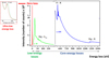 |
Fig. 9 A typical EELS spectrum acquired with 100 kV electrons through a MgO nanocube. It extends over 1500 eV and exhibits three major contributions : (i) in blue above typically 50 eV, the core energy-loss domain made of a regularly decaying background on which are superposed characteristic edges O-K and Mg-K; (ii) in green, from about 1 or 2 eV up to 50 eV, the low energy-loss domain which contains most of the intensity in an EELS spectrum; (iii), in red, the zero-loss peak now encompassing the ultra-low energy-loss domain which has only been explored with the latest generation of STEM instruments incorporating a monochromator. See text for discussion. |
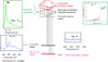 |
Fig. 10 Schematics along a vertical scale of energy of the origin and nature of the different excitations created in the electron population of the solid MgO by the high energy incident electrons. The parts of the spectrum selected in the different colour frames have been extracted from the energy loss spectrum shown in Figure 9: (i)bottom: individual atomic electrons excitations from core-loss levels, respectively O-K and Mg-K; (ii) collective (Pl) and individual interband transitions in the valence and conduction electron gas. |
3.1 Core-loss energy-loss domain (above 50 eV): inner-shell atomic levels excitations. Applications to elemental, chemical and electronic mapping with atomic resolution
Tables and collections of accessible edges for most elements and many compounds are now available in Egerton's book [56] and in reference libraries such as the EELS Atlas [www.eels.info/atlas] which is the EELS reference “bible”, and the EELS Data Basis [https://eelsdb.eu] which is currently updated with new spectra. The identification of these edges has now become an undisputable tool for qualitative elemental analysis of the atoms contained in a cylinder volume along the trajectory of the incident electron through the specimen thickness and the area section defined by the incident probe size. One step further, the measurement of the intensity of the associated signal combined to the knowledge of the relevant cross section σ is the key to the acquisition of quantitative elemental maps. This characteristic signal S(Δ) is measured over an energy loss width Δ following the threshold energy EC after background subtraction
 (1)
(1)
This integrated intensity is proportional to the number N of relevant atoms per unit area of the specimen:
 (2)
(2)
and I0 the incident beam intensity. The above formula practically becomes, as shown by Egerton [57]:
 (3)
(3)
where all quantities correspond to a limited angle of collection β and to a limited integration window Δ(eV) above threshold for signal measurement. This is the mostly used method for accessing quantitative elemental maps, with the support of calculations of atomic energy differential cross sections, based on the hydrogenic model [58] or on the more sophisticated Hartree-Slater method using a self-consistent atomic potential [59]. However, in certain cases, this procedure must be improved for instance when different edges significantly overlap or when a searched element is present in different chemical forms and therefore exhibits variable fine structures. In such situations, the whole spectrum can be supposed to be a linear combination of known reference spectra and a simple linear fit (often called Multiple Linear Least Square fit, MLLS) is then sufficient to determine the weight of each component in the experimental spectrum. This model-based quantification of EELS spectra such as accessible in Hyperspy [45], has been extended to include the fine structure of the characteristic edges [60] and consequently used to extend the analysis of SI from elemental to bond mapping in complex nanostructures [61]. A public software, EELSMODEL, has also been made available to solve issues of quantifying EELS spectra by model fitting (http://www.eeelsmodel.ua.ac.be).
With the access to corrected-probes down to the 0.1 nm diameter, 2D atomically resolved elemental maps have now become a common result following their first demonstration about 12 years ago in a bunch of papers [62–64]. In this last paper, the possibility of access to bonding maps through the information contained in the fine structures attached to an atomic edge was clearly pointed out. Today, this has become the preferred field of use of atomically-resolved core-loss EELS. In the following we'll therefore focus on the progress acquired in the recent years concerning these fine structures, their interpretation and their use to go beyond elemental maps into chemical and electronic maps (see review paper [65]).
As early as in our previous 1984 paper, recently republished as [18], these fine structures had attracted much attention. Many experimental spectra were shown, i.e. for the different phases of carbon solid or molecular (carbon K-edge) as well as for many solid oxides (O-K edges and TM L23 or RE M45 edges). Furthermore, preliminary paths to a satisfactory interpretation were indicated, emphasizing the importance of a local unoccupied density of states n (E, r) projected in space on the site of the core hole and in angular symmetry following the dipole selection rules (l' − l = Δl = ±1).
In order to extract maximum information from these fine structures, localized on threshold as well as in near-edge and extended oscillations, it has become obvious to compare the experimentally recorded EELS spectra with theoretical descriptions and their associated numerical simulations. Figure 11 summarizes the major routes, tools and software which have been developed over years to model, as finely as possible, these fine structures and their changes when moving the incident probe over areas of the investigated specimens. Depending of the symmetry of the final state, orbitals of s- and p- nature being more extended, of d- and f- nature being more localized on the excited atom, the best description is of solid state type (band structure) or of atomic type (multiplet theory). Between them, the calculation can be performed in the real space on clusters of atoms of more and more extended size from molecular orbitals to multiple scattering descriptions (ELNES and EXELFS, equivalent to the XANES and EXAFS in X-ray absorption spectra). Equivalently, the calculation of the local unoccupied density of states can be performed in the reciprocal space, in which case many codes have been developed most of them relying on the density functional theory DFT.
We can illustrate this with the simulation of the fine structures of the O-K (1s → 2p) and Fe-L23 (2p → 3d) edges in the simple case of the hematite iron oxide (α-Fe2O3) where the triple-charged Fe ion lies in a (distorted) octahedral Oh environment. A satisfactory starting point consists in calculating the MOs for this environment. The results [66] are shown in Figure 12b. The net result is that the oxygen 2p and iron 3d orbitals combine into crystal-field split t2g and eg levels separated by the ligand-field splitting energy 2.2 eV. Furthermore, as the iron oxides have ground states with high spin values, a calculation predicts that spin-up and −down electrons occupy orbitals separated by a spin-orbit splitting of 2.7 eV. Charge transfer and crystal symmetry within the first coordination shell are therefore essential to govern the fine structures observed on the pre-peak of the O-K edge (experimentally measured of 1.2 eV), as they correspond to transitions 1s→2p toward the oxygen 2p fraction in the unoccupied states hybridized with the 3d transition metal orbitals [67].
In order to push further the interpretation of the fine structures appearing on both edges [68], band structures calculations have been performed for the transition to the more delocalized unoccupied orbitals, as shown in Figure 12c, and the results of atomic-type approaches including the role of the core hole for the multiplet 2p63d5→2p53d6 transitions are shown in Figure 12a. They correspond to the extreme cases of calculation and associated software in Figure 11.
Another interesting case, which has been abundantly investigated over the past few years, deals with the O-K edge and the Ti-L23 edge in different oxides and perovskites. In particular, Radtke and Botton have published a review on the energy loss near-edge structures [69] which provides a good survey of the calculations, ab initio for the O-K and multiplet for the TM lines, compared with the experimental ones. For the different TiO2 phases, the valence does not change, the main variable parameter is the structural environment. Figure 13 illustrates how minute variations in the L3 and L2 lines corresponding respectively to the excitations of the 2p3/2 and 2p1/2 towards a final unoccupied orbital of d symmetry, can be monitored with a spatial resolution of the order of the interatomic distance (see also [65]). Individual spectra in the acquired spectrum-image were recorded within 10 ms and are rather noisy. But the addition of 8 × 8 of them over an area of 0.4 × 0.4 nm2 (i.e. equivalent to a unit cell size) exhibits a sufficiently high SNR to demonstrate a weak change of the Ti L3 line (increase of the split, weak asymmetric broadening, minor shift) across the interface (Fig. 13b). With the theoretical support of a combination of DFT within the local density approximation (LDA) and of charge transfer multiplet calculations, it can be shown that the observed gradual changes in crystal field splitting (reduction of 0.6 eV between STO and PTO) is induced by the tetragonal distorsion of the PTO cell with respect to the STO one (Figs. 13c and 13d).
Monitoring the evolution of these EELS edges, sensitive to both local charge on the cations (such as Fe2+, Fe3+, Fe4+) and site symmetries and crystal distorsions (Oh, Td,..), constitutes a unique tool to distinguish charge or structure changes with (sub)-atomic spatial resolution, when moving the electron beam on compound nanomaterials or recording their change in time under the electron beam. The charge (Ce3+ or Ce4+) on individual metallic rare earth ions encapsulated in neighboring peapod cages has been identified by Suenaga et al. [71] by comparing their M45 line shape and energy with reference spectra. Similarly, the valence state distribution of Mn3+ and Mn2+ in the parallel atomic columns in a Mn3O4 thin foil oriented along the [102] direction, has been mapped, with atomic resolution, through a fit of the position and energy position of their L3 line with a combination of reference spectra [72].
A similar example is the evidence of cationic and charge ordering in a complex transition metal oxide, an FTO (Fe1.35 Ti0.65 O3-δ) ilmenite thin film, by mapping the weight of the two components corresponding to the ++ or the +++ ionization in each L3 Fe line profile, as shown in Figure 14. It shows that Fe2+ is highly modulated with a higher contribution on the iron rich site with a ratio Fe2+ /Fe3+ of the order of 3:1, while Fe3+ is almost equivalent in intensity on both sites. The observed charge modulation is theoretically explained by Density Functional Theory with the introduction of oxygen vacancies between every metallic plane, thus giving access to an improved understanding of the magnetic and transport properties of these films [73]. In another complex oxide (Pb2Sr2Bi2Fe6O16) where diffraction studies show that the Fe3+ ions exhibit two different coordinations (6-fold octahedral and 5-fold tetragonal pyramidal), a similar analysis of the weak fine structures changes in the Fe L3 line profile, paves the way to atomic-resolved maps of the distinct oxygen coordinations around a Fe ion always trivalent [74].
These are a few examples of the potential richness of monitoring the changes of core-edge EELS fine structures to investigate the atomically-resolved charge and structural properties of bonds in complex structures.
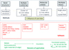 |
Fig. 11 Theoretical methods, software developed for the modeling of EELS fine structures on core edges, and their domains of applications (courtesy of Virginie Serin). |
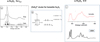 |
Fig. 12 A selection of theoretical routes used for the simulation of the relevant core edges (Fe L23 in (a), O K in (c)), compared to experimental spectra on a hematite α-Fe2O3 thin foil. They are respectively based on an atomic multiplet approach for Fe3+ ions and octahedral Oh crystal field of 2 eV (a) or on a band structure one in the DFT (Local Spin-Density Approximation (LSDA)) model (c). In (b), simplified description of the relevant MOs as an hybridization of the O-2p and Fe-3d atomic orbitals [66]. (figure with courtesy of Alexandre Gloter). |
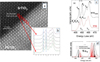 |
Fig. 13 Evolution of the Ti L23 edge across an atomically resolved SrTiO3(STO)/PbTiO3(PTO) interface (a) HADF image; (b) selection of six EELS spectra of the Ti L23 edge, each one built as the addition of 8 × 8 individual spectra recorded over the red squares shown in (a) [65]; (c) reference spectra recorded on larger areas of STO (black) and PTO (red); (d) ab initio and multiplet calculations of the L lines profiles demonstrating a reduced t2g-eg splitting of the L3 line from the cubic STO cell to the tetragonally distorted PTO cell [70]. |
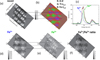 |
Fig. 14 Mapping the valence state distribution down to the atomic resolution in a ferrimagnetic hematite-ilmenite thin film : (a) HAADF image showing the position of the metallic atomic columns; (b) elemental map in false colors showing the position of the O atoms in red, of the Fe atoms in blue and of the Ti atoms in green; (c) EELS spectrum of the Fe L23 line in black on one metallic column displaying the presence of both Fe2+ and Fe3+ as it is made of the addition of both their signature with the corresponding weighted siderite (Fe2+) and hematite (Fe3+) signature; (d to f) Fe2+, Fe3+ and Fe2+/Fe3+ maps illustrating the charge order (from [73], courtesy Laura Bocher). |
3.2 Low energy-loss domain (from 1 to 50 eV): plasmons and interband transitions. Applications for the study of individual and collective electron excitations in the bulk, at surfaces and interfaces of nanostructures, mapping of electric fields
The electron energy-losses recorded in this spectral domain, often designed as Valence-EELS (or VEELS), actually constitute the dominant term in the spectra measured through a thin foil or at glancing incidence on surfaces or interfaces. In particular, since the earliest experiments such as in the Si thin foil shown in the introduction (Fig. 1, left), the most intense peak has been identified as due to the excitation of collective excitations of the quasi-free electron population of the material in strong Coulomb interaction. The physical properties of these bulk plasmons (energy dependence and angular dependence), have been extensively studied in the sixties and seventies, in particular by the group of Raether in Germany, see for instance [75–77]. These authors have also been involved in the introduction and broad use of the dielectric description, i.e. a phenomenological macroscopic approach using classical electrodynamics. The key quantity that accounts for the response of any material to an impinging high energy electron, is its dielectric response: ε(ω,  ) where ω is related to the energy loss by ΔE = ℏω and
  is the wave vector transfer. The inelastic cross section per incident electron for such a scattering event (ω,
  ) is related to the dielectric response by:
 (4)
(4)
where ε is a complex function that can be written as the sum of a real part and an imaginary part as: ϵ = ϵ1 + iϵ2. The real part ε1 describes a dispersion process while the imaginary part ε2 is related to electromagnetic absorption in the  limit. Equation (4) is the basic formula for the interpretation of electron energy-loss spectra in the low-loss region in bulk materials. A Kramers-Kronig transform can then be performed to extract ε1 and ε2 and the associated optical constants from the energy loss function:
  . When the collection angle is small enough and centered on the optical axis, the
  limit is reached and leads to the optical one. Simply speaking, collective excitations of the rather-free electrons of the material are to be associated with zero values of the ε1 curve while individual interband transitions from occupied to unoccupied states are responsible for strong bands of maxima in the ε2 curve.
These aspects have been extensively described in the past and in particular in the book of Ray Egerton [56] and in my two previous review articles dating back respectively from 1984 [18] and 1989 [78]. I will therefore focus now on the aspects of VEELS which have been most noticeably developed over the past few years: (i) individual transitions from unoccupied to occupied states and band gap measurements, and (ii) collective excitations at surfaces and interfaces.
3.2.1 Bulk VEELS spectra and band gap measurements
Let us start with the experimental contribution of VEELS to the knowledge of the whole excitation spectrum of the bulk solid made of different contributions (juxtaposition of individual electron transitions and collective ones) and with the theoretical background support developed to simulate them. As a typical example, Figure 15 shows the energy-loss function and its derived dielectric coefficients registered on a polycrystalline monoclinic-HfO2 powder sample.
This spectrum exhibits over an energy range from 5 to 60 eV, a lot of features to be related to the excitations of the complex electron population in such a compound. The conduction band is mostly made of Hf 5d states while the valence band is mostly made of O 2p ones. Semi-core localized electron states lying in the 10 to 30 eV range, and which can be involved in excitations over the energy range up to 60 eV, are the Hf 4f, O 2s and Hf 5p levels.
The bandgap onset is measured at 5.9 eV, the most intense feature is the bulk plasmon at 16 eV, which is located slightly above the energy where the real part of the dielectric constant crosses zero. It is followed by a series of high-energy interband transitions between 17 and 25 eV some of them involving O 2s electrons. At higher energies, the observed features have to be attributed to “semi” core-losses made of collective as well as of individual characters, the Hf O23 one being located above 33 eV. This simple description of the origin of the main features observed in the EELS spectrum and associated dielectric functions (Fig. 15), is further corroborated by detailed calculations performed within the frame of a time-dependent density functional (TDDFT) theory including local field (LF) effects [80], also previously used for the interpretation of TiO2 and ZrO2 EELS spectra [81,82].
In the insulators and semiconductors, the measurement of the bandgap energy Eg is of great value, it generally lies in the VEELS energy-loss range, it appears as the onset of the EELS spectrum intensity and of the associated absorption profile. As early as in 1971, Colliex and Jouffrey [83] in their EELS study of “rare solids”, i.e. solidified rare gases known as insulators of extremely broad gap, had identified peaks corresponding to excitons below the bandgap energy, interband transitions above bandgap followed by a maximum identified as a plasmon-type peak. For instance, in the case of solid argon the energy values of these different types of excitations are of 12.6, 16.9 and 19.6 eV in good agreement with values obtained in synchrotron optical reflexion experiments [84] and theoretical calculations [85].
Over the following decades, the combination of high energy resolution and high spatial resolution STEM-EELS has generated a number of bandgap and associated exciton and band structure measurements on a wide range of semiconductors and insulators. As a first example, Figure 16, due to Schamm and Zanchi [86] shows a few of these energy-loss Im (–1/ε(ΔE)) and absorption ε2 (ΔE)) curves for a selection of wide-band gap bulk materials, two oxides MgO and SrTiO3, and two nitrides BN and GaN.
Following Rafferty and Brown [87], the edge at the band gap can be fitted to a model (E − Eg)1/2 law for the case of direct vertical transitions between the top of the valence band and the bottom of the conduction band and to a model (E − Eg) 3/2 law for indirect tilted transitions.
Over the past two decades, there have been a number of experiments, in many cases supported by band structure calculations, aiming at recording VEELS spectra and measuring band-gaps in many materials of practical interest: BN filaments by Moreau and Cheynet [88], h- and c-GaN by Lazar et al. [89], YBCO with planar defects [90] and CdSe quantum dots [91] by Erni and Browning, h-GaN by Gu et al. [92], SiO2, SiNx by Park et al. [93]. In order to measure accurately the bandgap or onset of energy-loss, it is necessary to have a good model for the background of the zero-loss tail, and in this sense, the advantages of a monochromated primary electron beam has been fully demonstrated by Kimoto et al. [94].
As an example, Figure 17 shows some data recorded on YBCO and c-GaN thin foils. The fit of a square root function (E − Eg)1/2 to the upper part of the curve leads to a good measurement of the bandgap, respectively 1.35 eV and 3.2 eV.
However the task of measuring the bandgap with EELS in a precise manner suffers from some limitations. Some of them are associated to the fitting procedure and involve the choice of the model for the tail of the zero loss peak, which has improved noticeably with the use of monochromated beams radiation. However, for the extension of local band-gap measurements to band-gap mapping from spectrum-images recorded over areas with variable composition, new methods dealing with the necessary variations of the fitting parameter have recently been developed. They now lead to the automated extraction of bandgap maps with high spatial resolution [95].
Other limitations are fundamental and related to losses with energy below the onset of the bandgap transitions, such as Cherenkov radiation and associated guided modes generated by its total internal reflexion on the surfaces of the specimen. Practically, it has been noticed that the bandgap for specimens of increased thickness shifts towards lower values. It has been associated with the occurrence of Cherenkov losses. When the primary electron traverses a dielectric medium at a speed (v) greater than the speed of light in the medium (c/n), where n is the refraction index =  , it emits light, Cherenkov radiation, at the cost of energy loss. In an insulator, below the onset of the bandgap, ε2 (ω) = 0 and ε1 (ω) is positive and can noticeably exceed unity. This photon emission can be reduced by decreasing the value of the primary voltage, and consequently the speed of the electron. Therefore, for each semiconductor, with variable refraction index, there exists a critical high voltage below which Cherenkov radiation does not occur, which for most usual semiconductor is in the range 20–50 kV. Above it, a radiation peak is detected in the energy loss range for which ε1 (ω) > 1, typically between 2 and 4 eV, and in thick specimens can be of similar magnitude as the interband transitions. Therefore, it may be responsible for the observed shift of the onset of interband transitions. A positive point is that the scattering angle for electrons having generated Cherenkov radiation,
  rad, is very small and its contribution can only be detected at a small angle. Figure 18, extracted from [92] illustrates these two effects.
It has become obvious that with the gain in energy resolution due to monochromated electron beams, the generation of Cherenkov losses may bias the interpretation of spectra in terms of interband transitions and bandgap measurements. The use of thin specimens, lower primary voltages and large angle collection of the spectra is therefore recommended for judging the role of Cherenkov radiation, as demonstrated by Stöger-Pollach et al. [96].
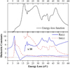 |
Fig. 15 Energy loss function and complex dielectric constants extracted from a Kramers-Kronig analysis of a deconvoluted EELS spectrum recorded on a powder of HfO2 (from Couillard et al. [79]). |
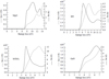 |
Fig. 16 Energy loss function Im (-1/ε)- black curves- and imaginary part of the dielectric function Im (ε)−dotted curves−near the bandgap for two oxides (MgO and SrTiO3) and two nitrides (h-BN and h-GaN), from Schamm and Zanchi [86]. |
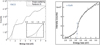 |
Fig. 17 VEELS spectra in the band-gap energy domain, after subtraction of the zero loss tail, showing how a fit with a square root function (E − Eg)1/2 can lead to a measurement of the bandgap. Intensity below this Eg energy can have different origins, such as the presence of surface defects quoted by the authors in the case of c-GaN (courtesy of Erni and Browning [90] for left figure and Lazar et al. [89] for right figure). |
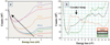 |
Fig. 18 VEEL spectra in h-GaN : (a) measured on specimens of increased thickness demonstrating the apparent band gap shift to lower values; (b) measured at different angles of scattering in a ω − q map, confirming the narrow angular distribution of the Cerenkov radiation (from Gu et al. [92]). |
3.2.2 Collective excitations at surfaces and interfaces
Bulk plasmons, i.e. collective longitudinal oscillations of the electron gas, have been identified since the mid-fifties, at the origin of intense narrow lines at multiple values of a quantized energy Ep, in the EELS spectrum of electrons transmitted through thin foils (see Fig. 1 left as a typical example). The value of this plasmon energy is Ep = ℏωp, with ωp the frequency of these charge oscillations being governed in a free electron gas model by its average bulk charge density, i.e. n ≈ 1028 e–/m3.

This value remains stable over spatially homogeneous specimens along the direction perpendicular to the electron beam and few studies have been devoted to monitor its variation when scanning the probe. A recent one [97] has demonstrated that monitoring the shift of the bulk plasmon energy can be used as a nanoscale thermometer, relying on the fact that the volumic mass density, and consequently n, varies with temperature.
Furthermore, boundary conditions, such as surfaces and/or interfaces between metallic and dielectric media generate localized surface charge oscillations, surface plasmons, which are associated with confined electric fields [77,98,99]. These excitation modes have been identified for a long time in the EELS spectra as features lying at lower energies (Es) than that of bulk plasmons, and appearing at a frequency (ωs) such as:

where εA (ω) and εB (ω) are the dielectric coefficients of the two media in planar contact. In the case of a free surface between the material A and vacuum, the solution occurs for εA (ωs) = –1 and in the free electron gas model,  . In a thin film of thickness smaller than the penetration depth of the fields, the charge oscillations on the top and bottom surfaces are coupled symmetrically or anti-symmetrically and generate in the EELS spectra, features known as (ω+) and (ω–). Their dispersion curves (ω,q) in the reciprocal space have been measured by Pettit et al. [100].
With the continuous progress in instrumentation over the past years (spectrum-images, sub-nm spatial resolution, high energy resolution in the 0.1 eV domain), it has become possible to record many EELS spectra at given positions in a specimen, such as defects, interfaces, surfaces, and to monitor their changes with improved accuracy in space and in energy, in particular for low-energy features generally superposed over the decreasing tail of the zero-loss peak. In particular these studies have blossomed with the spectacular success in creating nano-sized structures, such as clusters, nanoparticles, nanowires, nanotubes, offering a wide range of novel applications such as in electronics, catalysis, optics and requiring investigation of the local physical properties at the required scale. Figure 19 introduces a few of these geometries at the nm level for which, EELS has demonstrated its very rich ability to investigate with an unprecedented spatial resolution, well below the photon wavelength, the excitation spectrum and in particular the plasmonic response of these nanostructures. In the following we will address in more details each of the situations illustrated in the figure.
 |
Fig. 19 A selection of situations generating localized surface plasmons under the impact of the primary electron probe across them: (a) interface parallel to the beam; (b) nanowire, nanotube with axis perpendicular to the beam; (c) metallic nanoparticle of well defined shape supported on or protruding out of a substrate. |
3.2.2.1 Single or multiple planar interfaces oriented parallel to the electron beam
In the recent years, ultra-thin gate stacks made of different materials (metals, semi-conductors, insulators) have been grown to be active components in electronic devices of the latest generation. Their excitation spectrum under the impact of the primary beam has been monitored when scanning it across individual interfaces or a succession of them. The case of the Si-SiO2 isolated interface or inserted in a stack such as (Si/SiO2/HfO2/TiN) has been abundantly investigated over the past years. Very early, as visible in Figure 20, a bright line at about 8 eV (the interface plasmon IPl), just below the onset of the band gap edge at ∼9 eV in SiO2, is detected at the apex of the interface when the incident probe is scanned from the silicon to the silicon oxide. It lies significantly below the values of the bulk plasmons in Si (SiPl at 16.7 eV) and in SiO2 (SiO2Pl at ∼23 eV), at an energy ℏωs for which the equation.

As a matter of fact, the spatial profile of this IPl when the beam is scanned along the direction x perpendicular to the interface is rather wide, a few nm. A refined investigation has demonstrated a shift of this line from typically 7.8 eV to 6.8 eV when moving the probe from the interface to about 5 nm in the SiO2 [101], see Figure 21. This shift has been explained by considering relativistic effects, as illustrated in Figure 21b. The introduction in the model of a 1.0 nm thin layer of SiO has improved the agreement between experiment and simulation. It proves that the detailed structure of the interface can be of influence in the spatial and energy dependence of the interface plasmon mode.
As a consequence of the delocalized response of the interface to the incident electron probe, a nanometer scale layer structure such as a gate stack incorporating layers of oxide, semiconductor, metal, responds as a whole to the Coulomb field induced by the electrons traveling in one layer. As an example, the measurement of the bandgap of a 4.0 nm layer of HfO2, embedded between layers of SiO2 and TiN, respectively of 7.5 and 6.5 nm in a gate stack on a Si substrate, is obscured by the occurrence of the delocalized contributions from the interface plasmons, interband transitions and Cerenkov radiation generated in all layers of the investigated nanostructure [79]. These contributions originate not only from boundary conditions with the probed layer but also from the coupling of all interface modes in the system. These modes can couple up to distances of the order of v/ω, typically 10 nm. Simulations including relativistic effects, based on the methods developed by Bolton and Chen [102], predict very well these delocalized contributions. Similarly, Couillard et al. [103] in their study of the valence electron energy-loss spectroscopy of an ultra-thin SiO2 layer between Si stacks, have shown that, when the probe is located at the center of a 2 nm thick one, the response expected from a bulk SiO2 is suppressed and the delocalized contributions dominate. They point out that it raises a significant challenge when one aims at extracting local optical properties of ultrathin layers by electron energy-loss spectroscopy.
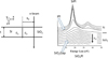 |
Fig. 20 Monitoring the appearance of the Interface Plasmon IPl in a thin foil of thickness (t) when the e-beam is scanned over a Si/SiO2 interface oriented parallel to the beam trajectory. |
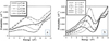 |
Fig. 21 (a) Experimental variation of the Si/SiO2 interface plasmon (IPl) peak profile when the position of the e-beam with respect to the interface (x0) is varied from Si (x0 < 0) into SiO2 (x0 > 0); (b) Theoretical calculations in the non-relativistic and in the relativistic case (R) for different probe positions (x0 = –1, 2 and 5 nm), from [101]. |
3.2.2.2 Single or multiple spherical or cylindrical surfaces or interfaces
For spheres, the excited surface modes are indexed as a function of their angular momentum quantum number l in spherical coordinates, l = 1 being the dipolar one. Practically, it is established [104,105] that:
for a metal sphere in vacuum, the surface plasmon frequency is: (ωs)l = ωp/[(2 l+1)/ l]1/2 which increases from ωp/√3 for l = 1 up to ωp/√2 for l → ∞
for an empty sphere in a metal (void, bubble): (ωs)l = ωp/[(2l +1)/(l +1)]1/2 which decreases from ωp/√(3/2) for l = 1 down to ωp/√2 for l → ∞.
In the quasi-static approximation, the energy of the different modes does not change with the radius of the particle, but with the position of the beam with respect to it. For glancing incidence, all modes are excited with their probability varying as 1/l, while only the dipolar mode is excited far from the outer surface. In the case of concentric spheres of different natures, such as a core of radius R1 covered by a layer of thickness t, the surface modes can couple. In the case of a conducting surface coverage or a thin metallic spherical shell, it induces a shift and a resonance splitting of the resonant frequencies, the more important as the thickness is smaller. The case of the surface- and interface-plasmon modes on small semiconducting spheres (Si/SiO2) has been fully investigated by Ugarte et al. [104]. In particular, to improve the agreement between experiments and simulations, the authors have introduced the presence on the external surface of the silica, of a supplementary ultra-thin conductive layer (likely reduced SiOx) responsible of the appearance of an extra line at 3–4 eV precisely localized on the external surface of the oxide layer.
In the case of an elongated sphere along one direction corresponding to an ellipsoid, the dipolar mode of the sphere is split into two modes, a transverse one (T) with the electrons oscillating perpendicularly to the long axis and a longitudinal one (L) with the electrons oscillating parallel to it. The resonance energy of the T mode is close to that of the equivalent sphere, which is 2.4 eV for an Au nanorod and 3.5 eV for an Ag one. As for the L mode its resonance energy is shifted towards lower values depending on the aspect ratio (L/D) of the particle, L and D being respectively the length and the diameter of the cylinder. This splitting into two modes is clearly visible in Figure 22a, from [105], which shows calculated and experimental STEM/EELS spectra for two probe positions at glancing incidence on an Au nanorod of aspect radio of the order of 3. For longer rods and associated higher aspect ratios, the longitudinal modes result from the combination of surface plasmons propagating in the two opposite directions into standing waves with a succession of quantized nodes and antinodes with n = 1, 2, 3…, see Figure 22b, from [106]. The energies of these longitudinal modes are much and much lower as the length of the nanowire, and therefore its aspect ratio, increases, as it is visible in the right part of Figure 1 illustrating the newest possibilities of EELS in a monochromatized STEM. As for the transverse mode, it is visible in the high energy part of the spectrum, close to the energy of the bulk.
A special family of cylindrical nano-objects which have gained a particularly high level of interest from the mid 90s are the nanotubes made of concentric layers of 2D material, such as carbon, BN, transition metal dichalcogenides. In such cylinders of infinite length, one is interested by the radial distribution of oscillating charges on both inner and outer surfaces. Furthermore, these layered materials exhibit strong anisotropic properties with a dielectric coefficient being a tensor rather than a scalar, with two main coefficients ε‖ and ε⊥ where ‖ and ⊥ correspond to the geometrical configuration with respect to the c axis of the structure, and therefore to the out of plane and to the in plane directions of the atomic layers.
The advantage of the STEM/EELS experiment is that it connects directly the occurrence of well-identified features in the spectra, to the spatial location of the incident probe with respect to the nanotube, through the bulk of the nanotube, at glancing incidence on the inner and outer surfaces or in vacuum at an impact distance from the tube surface. For relatively thick nanotubes, the observed peaks resulting from collective excitations of the valence electrons can be directly deduced from the well-known bulk excitations in planar graphite : the peaks respectively at 6 and 25 eV are respectively generated by collective excitations of the electrons of π and of π + σ characters, while surface modes at 6, 13 and 17 eV, are detected for non-penetrating beam positions up to large impact parameters [107]. A refined study of the origin and characteristics of these excitations in thin carbon nanotubes made of a small number of layers down to 1, has demonstrated besides the sharpest line associated to the excitation of the π plasmon at 6 eV, the existence of two surface modes implying π- and σ-electron excitations at 15 and 19 eV respectively. With the support of simulations performed in the framework of the continuum dielectric theory accounting for the local anisotropic character of the nanostructure and adapted to a hollow cylindrical object, it has been shown that a key parameter influencing the shape and relative intensity between these peaks at 15 and 19 eV is r/R, the ratio between the inner and the outer diameters of the nanotube [108]. This is clearly visible in Figure 23 which shows the good agreement between experiment and theory in this case of strong coupling between the two surface plasmons giving rise to a tangential mode and to a radial mode. The first one is associated to similar charges on the facing inner and outer surfaces and associated electric field lines parallel to them while the second one is associated to opposite charges on the facing surfaces and associated electric field lines perpendicular to them. In the limit case of a single carbon layer, only the first mode, the tangential symmetric one remains while the radial antisymmetric one disappears.
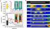 |
Fig. 22 STEM/EELS maps on a metallic nanorod: (a) calculated probabilities and experimental spectra and locations of the transverse (T) and longitudinal (L) surface plasmons measured at positions A and B close to a short Au nanorod (L/D = 85 mm/27 mm), from Chu et al. [105]; (b) STEM/EELS maps for an Ag nanowire of aspect ratio of the order of 30, showing the spatial distribution of 6 first order n = 1,…,6 longitudinal modes at energies between 0.5 and 2.3 eV, while the transverse modes covers rather homogeneously its whole length, from Rossouw et al. [106]. |
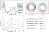 |
Fig. 23 Experimental EELS spectra recorded at grazing incidence on C nanotubes with different numbers of layers and associated r/R ratios (bottom curves) and simulated ones (top curves). The split peak at 15 eV corresponds to a tangential mode with field lines parallel to the surfaces of the nanotube and at 19 eV to a radial mode with field lines perpendicular to the surfaces of the nanotube. One notices the vanishing of the radial mode for the single-wall nanotubes (from Stéphan et al. [108]). |
3.2.2.3 Plasmons on nanoparticles of various shapes and sizes, an introduction to nanoplasmonics
The strong correlation between the movement of charges and the generation of electromagnetic fields, such as illustrated in the previous paragraph in the case of metallic nanorods and thin carbon nanotubes, has generated the growth of abundant experimental and theoretical studies. In the moderate energy-loss domain corresponding to an optical spectral window from the IR to a rather far UV (typically from 1 to 20 eV), EELS spectra exhibit peaks and features attributed to collective excitations of the more-or-less free electron gas of the material, plasmons. Boundary conditions, such as surfaces or interfaces between metallic and dielectric materials, generate localized or propagating surface charge oscillations, surfaces plasmons (SP) associated with electric fields. Their mapping at an unraveled sub-nm spatial resolution has become a field of intensive research in the context of the development of techniques creating nanostructures of various shapes and sizes, one of them being in the nm-range for use in many different domains such as electronics, chemistry, mechanics and energy production. In particular, the burst of interest for metallic structures and devices guiding, enhancing and controlling light at the sub-wavelength has generated the birth and rapid growth of “nanoplasmonics”. Many groups, all over the world and in particular the Orsay STEM one, have been very active over the past fifteen years, in the domain of EELS mapping of propagating surface plasmon polaritons (SPP) and localized surface plasmons (LSP), more and more in connection with the mapping of the associated desexcitation photon signal measured by an optical spectrometer, i.e. cathodoluminescence (CL). A few recent reviews have recently been published [109–112], providing detailed surveys of this blooming field of nanoplasmonics. In the present text, only a few key features will be addressed.
Practically, many types of nano-objects, made in majority of Ag or Au and more recently of Al, Cu, have been fabricated with different shapes (1D nanoantennas, 2D flat prisms, 3D nanocubes, star-shaped, disordered…), using bottom-up (colloidal chemistry) or top-down (lithography) techniques. In the electron microscope, the incident electron beam is scanned over a random or organized distribution of these nanoparticles deposited on a thin insulating support layer of bandgap sufficiently large not to overlap with the metallic plasmonic structures under investigation (for instance mica, Si3N4…). A collection of EELS spectra, in practice a spectrum-image, is recorded, so that maps of the generated features (energy, intensity, width) are produced. Beyond the nanorods, already mentioned above, the triangular silver nanoprism of constant thickness, has constituted a seminal case to experimentally identify the major excitation modes and to test their theoretical modelling [113–115]. Figure 24 shows the major trends of the analysis of the spectrum-image recorded on the single silver platelet of 78 nm edge length and 10 nm thickness imaged in the ADF mode. Three distinct modes are clearly visible with the lowest energy one at 1.75 eV localized at tips (spectrum A), the medium energy one at 2.70 eV along the edges (spectrum B) and the high energy one at 3.20 eV roughly in the center (spectrum C).
The origin of the observed features in these EELS spectra has to be related to the electromagnetic eigenmodes generated by the impinging swift electron on the metallic nanoparticle. The measured energy loss actually corresponds to the work produced by the primary electron of velocity v travelling through the induced field Eind which it has generated, and it is of the type (v.Eind). Therefore, only the z component of this induced field (Eind)z along the trajectory of the electron comes into account. To calculate it for quite different morphologies and sizes of nano-objects, numerical approaches have been elaborated for solving the relevant Maxwell equations and consequently for simulating maps of the energy and intensity of the EELS peaks. One of them, the boundary element method (BEM), relies on a discretization of the interfaces (r) and calculates from an integral equation involving the surface charge densities, the maps of the eigen-potentials Φi(r) and eigen-electric fields Ei(r), and then the induced EELS maps. This technique has been used in [113] to interpret the tip and edge modes observed in Figure 24 as eigenmodes of the associated electromagnetic fields respectively of dipolar and quadrupolar types, see Figure 25a. The 0.2 eV slight difference between experimental and simulated resonance energy is attributed to the rough experimental estimate of the thickness of the silver nanoprisms. A definite progress in the mathematical description of surface plasmons in a wide panel of nanostructures within this BEM approach is due to Hohenester and Trügler [116] who have developed a software (MNPBEM), that is a Matlab well adapted to the simulation of theoretical maps to be compared to experimental ones.
An alternative method for the simulation of surface plasmon maps is the Discrete Dipole Approximation (DDA), which accounts for the volume of the particle as a discrete number of polarizable volume elements [117] instead of the surface charges. In [114], the agreement between the experimental and DDA simulated dependence of the surface plasmon resonances of triangular platelets as a function of their aspect ratio R = L/t (where L is the edge length and t the thickness) has been fully demonstrated. In this study, it has been demonstrated that the energy of the tip and edge modes globally shifts to lower values when the lateral dimension L increases and that in fact the aspect ratio is the key factor. For bigger nanoprisms of increased thickness significantly larger than the skin depth of electric field penetration in the material, the electric coupling between the two horizontal surfaces is negligible. Then, surface plasmon polaritons similar to those in nanorods propagate along the wedges giving rise to stationary waves with increased numbers of nodes and antinodes (n = 0, 1, 2, 3, 4). These numbers of plasmon intensity maxima have been observed between 0.6 and 1.6 eV along the 950 nm long edges of an Au prism of thickness t = 70 nm [115].
A recent detailed EELS study of plasmon mapping on aluminum equilateral triangles of 40 nm thickness and 125 to 700 nm edge legth deposited on a 30 nm thick Si3N4 membrane, has provided a further insight into the observed complex patterns [118]. The experimental high resolution imaging and spectroscopy of excitation modes recorded on a wide spectral region from the IR to the UV display a number of features which can be ascribed to edge modes (E) concentrated along the boundaries of the triangle and pseudo-radial breathing ones (RBM) concentrated inside the triangle cavity (see Fig. 26).
When compared with the three major LSPs (tip, edge, center) identified by Nelayah [113] on an Ag triangle of smaller size, this experiment has revealed a much more complex and richer set of spectra and plasmon intensity maps. Along the boundaries, the spectra exhibit edge modes indexed as E1 to E5 between 1.02 and 2.66 eV, E1 being dominant at the tip and E2 in the middle of the edge. These edge modes are similar to the surface plasmon modes on linear antennas of the same length, such as those shown in Figure 22b. As for the spectrum recorded in the center of the particle, it shows over the energy range from 2.5 to about 4.0 eV a series of bumps indexed RBM3,6 to RBM5,10. Intensity maps of these bumps fitted with gaussian functions exhibit characteristic patterns, which are ascribed to “breathing-like” surface plasmon modes SRSPs, which propagate on the surface of the particle and are sequentially reflected on their edges. With reference to optical considerations, these modes arising from the constructive interference of propagating waves are indexed within a 2D Fabry-Perot description as the edge-ones are also indexed along a 1D Fabry-Perot description. Novel simulations techniques have recently been elaborated to be used for the interpretation of different combined electron/optical techniques. In particular, several aspects of the interaction of fast electrons with nanostructures producing electron energy-loss (EELS) and cathodoluminescence (CL) signals can be described using a generalized field propagator. The 3D-Green dyadic method (3D-GDM) is well known in the optics community to be quite adapted to the description of the optical properties of nanostructures of arbitrary geometries. It has been shown by Arbouet et al. [119] that this method can yield the EELS and CL of nano-objects of complex morphologies embedded in different dielectric media. In the study by Campos et al. [118], the experimental intensity maps of the E and RBM modes in Al triangular prisms are quite positively compared with extensive electrodynamical simulations performed using the GDM approach, see Figure 25b.
Beyond these 2D-platelets, 3D nanostructures and in particular nanocubes, have also been extensively investigated. In the continuation of the results obtained on lower-D nano-objects, they exhibit corner, edge and face modes. Furthermore, optical experiments and theoretical studies had also revealed the role of the substrate, responsible of the splitting of the peaks into “proximal” and “distal” components in direct contact with the support or on the opposite face [120]. A refined 3-D EELS mapping of the localized surface plasmon resonances (LSPR) on a silver nanocube combining spectrum-images, tilt series and specific data processing for tomographic reconstruction, has been performed by Nicoletti et al. [121]. It confirms the existence of corner, edge and face modes all of them exhibiting the dual proximal and distal character, see Figure 27.
Another interesting category of 3D-nano-object, without symmetry, are star-shaped with a central spheroid out of which protrude in random directions, individual arms of variable shape, length and tip radius. A STEM-EELS study [122] on a set of such gold nanostars has shown that they generally display two types of LSPRs, one around the central core quite similar to the dipolar mode of a sphere and another one localized at the tips with energies depending on the local topography and curvature. These modes at the end of the star arms are weakly coupled between them and are induced by local field enhancements.
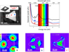 |
Fig. 24 Maps of the three major localized surface plasmons (LSP) recorded at positions A, B, and C on a silver triangular nanoprism shown in the HADF image, together with the relevant EELS spectra. Spectrum D is recorded outside of the prism, on the substrate as a reference. The rainbow illustrates the energy position of these excitations with respect to the visible spectrum (from [113]). |
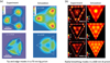 |
Fig. 25 Comparison of experiment and simulation for the interpretation of LSP modes recorded on metallic triangle prisms of different nature and size : (a) 70 nm Ag prism (courtesy J. Nelayah et al. [113]), (b) 600 nm Al prism (courtesy A. Campos et al. [118]). |
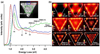 |
Fig. 26 (a) Deconvoluted EELS spectra recorded at different positions (tip in red, edge in blue, center in green) of a 604 nm side long Al nanotriangle; (b) intensity maps of the different plasmons of edge (E) and radial breathing (RBM) nature identified in the spectra (from Campos et al. [118]). |
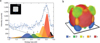 |
Fig. 27 3D-EELS tomographic mapping of the localized surface plasmon resonances (LSPR) on a 100 nm silver nanocube deposited on a 30 nm thick silicon nitride substrate: (a) EELS spectrum recorded for the probe position marked in blue on the HADF image and identification of the spectral components (α, β, γ, δ, and ε) to be attributed to LSPRs on the cube, also visible are the zero-loss tail and the bulk silver plasmon (in black); (b) the reconstructed 3D map of the identified specific components (from Nicoletti et al. [121]). |
3.2.2.4 Hybridization of modes and quantum limit
Real systems developed for practical applications in nanophotonics for instance, are made of several nano-objects, from a couple to a whole set of many similar ones. It is therefore important to understand how such nano-devices can handle light at the smallest scale. Spatially-resolved EELS is quite useful in this field.
Consider the simple case of a dimer made of two closely spaced metallic nanorods: when the distance between them is shorter than the decay length of the electric field perpendicularly to their outer surface (typically up to a few tens of nm), the electromagnetic interaction leads to the mixing, or hybridization, of the LSPRs on the individual components, inducing splitting and shifts of the plasmon energies as illustrated in Figure 28. Introducing a strong analogy with the hybridization of molecular orbitals, Prodan et al. [123] have described the origin of the “bonding” modes as due an asymmetric distribution of charges on facing nanorod ends and consequently a strong finite dipole moment along the line between their centers. This mode can easily be excited by light, but is invisible in STEM EELS because the associated electric field  is perpendicular to the velocity of the incident probing electrons. On the opposite, when similar charges cover facing ends, the “antibonding” modes are optically dark because there is no dipole across the gap, but are most intense in an EELS measurement, as confirmed by the experiment in Figure 28b. Similar observations have been realized for homo- ad hetero-dimers of spherical nanoparticles [124], of split nanowires [125] and of triangular platelets in bow-tie configuration [126].
The limiting case of ultra-narrow gaps, typically below 1 nm, between two metallic surfaces (tips, spheres) down to contact when the nanostructures are joined with a bridge of increased width, has been experimentally and theoretically investigated. In their study, Kadkhodazadeh et al. [127] manipulate small silver nanoparticles with the electron probe and record the change in the EELS spectra during their approach until contact. They observe the transition in the system plasmonic response from the “classical” bright and dark dipolar plasmon mode into a “quantum” charge transfer plasmon mode appearing when the surfaces are very closely spaced (0.3 nm). This new mode is associated to a tunneling regime where the electron transfer neutralizes the huge surface charge densities on the opposite faces of the junction. Once contact occurs, a charge transfer plasmon mode occurs at lower energies as a precursor of a dipolar plasmon of the whole pair of nanoparticles. The bridging of these “classical” and “quantum” modes has been theoretically described in a quantum-corrected model that incorporates quantum mechanical effects within a classical electromagnetic framework [128].
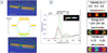 |
Fig. 28 (a) Hybridization of the basic dipolar surface plasmons between two adjacent nanorods : (Center) Energy splitting of the fundamental mode of a dimer antenna with the corresponding charges distribution and electric field lines in the bonding (bottom) and antibonding (top) modes; (b) EELS spectra and intensity maps on a silver nanorod dimer demonstrating the appearance of the bonding and antibonding modes : the first ones at lower energies (1.2 eV) peak at the outer extremities of the dimer (spots in positions red and blue), the second one of stronger intensity and higher energy (1.35 eV) peaks right in the gap between the rods (spot in position green). Each silver rod is 40 nm thick and 200 nm long (courtesy Z. Mafoud, Ph.D. Orsay, 2012) |
3.2.2.5 “Nanoplasmonics”, a rich field of applications for photonics issues
Plasmonics is the science and technology of the interaction of light and metallic objects. Within this huge field of potential applications, localized surface plasmons (LSP), collective oscillations of the electron gas, can generate and manipulate electromagnetic fields at a scale significantly below the optical diffraction limit. Therefore, their detailed investigation at their ultimate spatial and spectral scale, i.e. “nanoplasmonics”, opens new routes in photonics, with clear developments not only in optical devices but also in catalytic routes or cancer therapy.
The role of EELS in a STEM to explore the optical response of a nanostructure with ultimate spatial resolution has been extensively described by Garcia de Abajo [109] in his very comprehensive review on the optical excitations explored in an electron microscope. In particular, the spatially resolved EELS and CL (cathodoluminescence) techniques are the alternative methods to reach this goal, best spatial resolution with EELS and best spectral resolution with CL. Furthermore, the theoretical tools which are necessary to interpret the acquired experimental spectra have reached a mature status as well in the frame of the classical dielectric approach as in the quantum mechanical description.
In order to illustrate schematically how electrons and photons can be associated to excite and detect the plasmonics response in a nanostructured material, let us have a look at Figure 29. A simple argument bringing together electron inelastic scattering and photon absorption and scattering lies in the schematics of generation and detection of the signals generated under the impact of a swift electron or of a photon pulse on a nano-sized metallic object [129]. Figure 29 (left) is a simplified representation of the interaction between an incident electron of high energy travelling in the vacuum at a distance of a few nm outside the external surface of an isolated metallic particle of diameter in the 10 to 100 nm range. This swift point charge can be regarded as a source of white light, which induces the oscillation of charges in the object, i.e. the creation of a LSP, with a resonance frequency depending on its nature (through its dielectric constant ε), its shape and its size. This surface plasmon generates an evanescent induced field, which the electron travelling at velocity  feels, thus giving rise to an energy loss measured by the electron energy loss spectrometer (EELS). The induced EM field can also be directly detected by an optically coupled spectrometer and photon detector, in which case the signal is named cathodoluminescence (CL).
An alternative way to stimulate the creation of LSPs on a metallic nanoparticle is to shine it directly with a photon beam (Fig. 29 right). The induced evanescent field can also be detected by a swift electron travelling aloof the particle or directly with the photon spectrometer-detector device (in this case, this is a photoluminescent signal and there is no spatial resolution at the nm level). As the decay time of the plasmon (on the 10−15 s scale) is much shorter than the time elapsed between the arrival of two electrons (10−9s), it is necessary to correlate in time both photon and electron impacts. This direct visualization of near-EM fields (called PINEM for photon induced near-field electron microscopy) has been beautifully demonstrated by the group of Zewail [130,131], who have used ultra-fast electron microscopy techniques in a pump-probe approach. However, beyond the demonstration of a strong imaging process between inelastic electrons and photons produced by LSPs, this approach does not provide rich information on the specimen. This is why the remaining part of this paper will be devoted to the discussion of multi-signal STEM approach.
The link between EELS and CL has been investigated through the comparison of their data output when realizing the experiments on the same object in the same STEM microscope equipped with an EELS spectrometer/detector and CL spectrometer/detector [132]. Figure 30 shows the spectra recorded on a small triangular nanoprism (60 nm side length) on a graphene thin layer (left) and on a larger one (140 nm side length) on an amorphous carbon film (right).
The data sets, for each individual particle, have been acquired sequentially because the experimental illumination conditions are very different for both spectroscopies, the acquisition of a CL spectrum requiring a beam current typically two orders of magnitude higher than for an EELS one. This experiment shows that the two spectroscopies reveal the presence of a major dipolar mode at the tips of the particle with the same energy. More generally, these combined measurements on the same particle confirm that CL detects only radiative modes while EELS also shows dark modes. When considering the larger particle, the dipolar EELS resonance is significantly blue-shifted with respect to the CL one. This shift occurs because EELS measures the energy lost by the fast electrons interacting with the particle, whereas CL measures the part of this energy radiated into the far field, and is related to the damping mode.
The role of EELS (and CL) to probe the optical properties of nano-objects is further confirmed when comparing their output with cross-sections involved in far-field optical experiments. When one sends an optical plane wave onto a NP, it can be absorbed or scattered with the probability of occurrence of these events governed by the associated absorption and scattering cross sections. The extinction cross section is the sum of the two previous cross sections and it accounts for all interaction of the light beam with the NP and it is measured as the decrease in intensity of the light beam. Simulations show that spectral differences observed between EELS and CL are also present in light extinction and scattering, confirming that spectral differences observed as a whole in far-field spectroscopies are maintained in the nanoscale observation of individual particles by EELS and CL [132,133].
At this point, it is interesting to emphasize the connection between the local excitation of surface plasmons, i.e. of surface charge oscillations generating electromagnetic fields as schematically shown in Figure 29, and the electromagnetic local density of states (EMLDOS), as proposed by Garcia de Abajo and Kociak [134]. This local density of states represents the probability of finding a given EM mode at a given point in space and at a given energy. Practically, it is shown that EELS and CL are closely connected to the projection of this density along the z-axis, i.e. along the direction of movement of the electric charge, the z-EMLDOS. It definitely brings EELS and CL closer to photonics. However, the practical reconstruction of plasmonic results in terms of LDOS has remained challenging for a while. Hörl et al. [135,136] have developed a route for retrieving the three-dimensional local photonic density of states around nanocubes or coupled nanodisks, through the solution of an inverse problem starting from a combination of angularly tilted EELS spectrum-images.
There is no surprise that the combination of these two techniques EELS and CL probing electron excitations and accompanying electromagnetic fields at the sub-nm level and covering a spectral domain significantly broader than the visible range, have established themselves as key routes into the exploration of the rapidly expanding domain of nanophotonics.
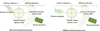 |
Fig. 29 Schematics of the generation and detection channels for localized EM fields induced by an impinging swift electron (left) or a photon beam (right) on a metallic nanoparticle |
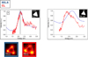 |
Fig. 30 Left : EELS (solid blue line) and CL (solid red line) spectra recorded at the tip of a single gold triangular nanoprism (60 nm side length) using a STEM. EELS and CL maps of the intensity of the resonance peak in the spectra are shown respectively inserted in blue and red frames. (Right) : for the larger particle (140 nm side length), the CL resonance is shifted compared to the EELS resonance, showing that the dipolar plasmon mode resonates at different energies in CL and EELS (reproduced and adapted from Losquin Ph.D. thesis Orsay (2013) and [132]). |
3.3 Ultra-low energy loss domain (under 1 eV): electron excitations in the IR domain, phonon modes
As a matter of fact, this ultra-low energy loss domain corresponding to the IR electromagnetic spectral range, has been extensively investigated with different vibrational spectroscopies using photons ((infrared optical, Raman) or neutrons as primary particles. As for the use of electrons, the energy resolution which they offer in this energy-loss range has remained limited for years and their contribution has mostly been concentrated in techniques relying on primary slow electron beams scattered at surfaces in the reflection geometry, see [137] for a review. However, as early as in the sixties, Boersch et al. had built a combination of monochromator and spectrometer which could measure energy losses of primary 20 to 30 kV electrons through thin foils with an energy resolution of about 10 meV [4]. EELS spectra showing lines attributed to the excitation of surface lattice vibrations in LiF at 50 meV were recorded with this instrument [138]. Later on, full spectra through an evaporated germanium film exhibiting signals corresponding to phonon, Ge-O bonding and intraband transitions between 30 and 200 meV were published [139]. However, this potentially rich domain of research has not been actively explored over the following decades, mostly because its restricted spatial resolution. Therefore, the recent introduction of monochromators offering an energy resolution below 10 meV (see Fig. 3), has definitely opened with the high spatial resolution offered in the new generation of STEM microscopes, the exploration of new types of excitations, the observation of which was traditionally hidden in the large energy tail of the zero-loss peak. It is therefore no surprise that a flowering bunch of papers dealing with the excitation of electrons in molecular bonds or of vibrations of the ions, has come out over the past few years. In the following, I will introduce three typical examples of studies presently under development.
3.3.1 Surface collective electron excitations in the sub-1 eV energy range
In the introduction of the present review, the jump in accessible energy range offered by the new-monochromatized generation of STEMs was illustrated with a comparison between bulk plasmons in Si thin foils (recorded in the seventies) displaying six eigen modes over 100 eV and surface plasmons in long Cu rods (recorded last year) exhibiting 25 eigen modes over 1 eV. In a search for nanostructures able to significantly enhance local electromagnetic fields, systems of high quality factor Q defined as the ratio between the absolute energy of the plasmon mode and its width, or the product of its frequency and lifetime (Q = ω · τ), are very desirable. It means plasmon peaks as sharp as possible with weak damping and therefore long lifetime. Using a monochromatized beam of typically 60 meV, Bosman et al. [140] have recorded plasmon peaks on different positions on gold nanoresonators of rod or cross shapes with sufficiently high SNR to measure accurately their width. For structures between 25 and 35 nm in diameter, the Q factor of peaks ranging between 0.5 and 2.5 eV has been shown to be maximum around 20, in good agreement with theoretical simulations.
In an effort to find materials and nanostructures exhibiting high quality factors, Mkhitarian et al. [141] have investigated the properties of mid-IR plasmon modes on elongated Cu nanorods compared with those of Ag counterparts. They have used high resolution EELS to spectrally map plasmons down to below 100 meV domain on copper and silver nanowires of length up to >10 μm. Figure 31 shows with an energy resolution of 10 meV and a spatial resolution of 1 nm the distribution of plasmons of different quantum numbers n along a Cu nanorod of 3.15 μm length. In this detailed comparative study of Cu and Ag nanorods of length up to about 20 μm, EELS spectra displaying high numbers of plasmonic modes have been recorded, for instance n = 28 at 1 eV, at the tip of the 15 μm Cu nanowire (bottom spectrum of Fig. 31b).
A comprehensive analysis of the FWHM of the different plasmon peaks, after deconvolution, background subtraction, has shown that very low plasmon energies down to <20 meV can be observed in the mid-IR and high quality factors up to 60 measured in the visible part of the spectra. Copper is thus shown to be a competitive metal with silver to generate long-living localized plasmon modes, this is a consequence of the localization of their electromagnetic energy largely outside the rods thus reducing the role of the inelastic losses in the material itself.
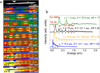 |
Fig. 31 Infrared plasmons in long Cu nanorods: (a) maps of the different modes with n increasing from 1 to 10 for a Cu rod of length L = 3.15 μm, diameter D = 121.1 nm, and AR = L/D = 26 (see its ADF image on top). The number of nodes on each of these maps is equal to n + 1, in the middle of these rods there are visible peaks only for n is even; (b) plasmonic EELS spectra collected near the tip of Cu nanorods of different geometrical parameters L, D and AR. A spectrum collected in the middle of the rod displays only peaks of even number n, shown as a dashed plasmon spectrum (from Mkhitarian [141]). |
3.3.2 Vibrational modes in molecules and nanoparticles
Vibrational spectroscopies such as inelastic neutron and X-ray scattering, Infrared-spectroscopy, Raman scattering, inelastic scattering of low-energy electrons or inelastic electron tunneling on surfaces, provide a lot of rich information on the collective vibrations of ions in crystals or surfaces, on molecular bonding arrangements, which are all quite essential in our understanding and control of many physical properties of solid materials. However, these techniques provide accurate measurements on volumes and surfaces above the micron range in most cases, and are of limited impact for studying these properties in the nm range and therefore when studying nano-objects down to the single atom.
Therefore, the access to the IR spectral domain, typically from 10 to 500 meV, with a monochromated EELS-STEM, has largely opened in the recent years the study and mapping of vibrational modes with the required high spatial resolution. In their paper demonstrating the richness of the spectral information revealed in the tail of the zero-loss peak when closing the monochromator slit down to a typical 10 meV value, Krivanek et al. [19] show vibrational signals from various materials prepared as thin foils, such as that one at 173 meV to be attributed to the LO-phonon in h-BN. It also points out the possibility of detecting EELS peaks corresponding to vibrational stretch energies of bonds involving H atoms such as H-C, H-N, H-O. Another important point carried in this paper is the demonstration, by imaging the variation of the SiO2 optical phonon at Si/SiO2 and SiO2/vacuum interfaces, of the double level of spatial resolution carried in these experiments: (i) high at the nm scale, (ii) low in the “aloof” geometry when the incident beam travels at a large distance (between 10 and 40 nm) from the specimen edge.
This duality of accessible spatial resolution has been further investigated by Dwyer et al. [142] in a series of measurements and associated calculations of the vibrational modes detected in a STEM-EELS experiment on a thin h-BN foil. They confirm the existence of a “dipole delocalized” scattering of the phonon signal (generally of the LO type) detectable at small momentum transfers and scattering angles, when the electron beam travels at a distance from the specimen edge up to hundreds of nm in the vacuum. In parallel, a “localized” vibrational signal, of reduced intensity, is detected when collecting electrons passing close to an atomic ion and scattered at large angles or with large momentum transfers in the diffraction pattern. This off-axial geometry can then be used to map vibrational modes of a material with a spatial resolution of the order of one nanometer.
The detection of the “dipole delocalized” mode at a distance from the specimen has been advocated [143] and demonstrated [144] as a unique opportunity to map without observable radiation damage, the distribution of the stretching modes of molecular bonds and therefore of significant molecules in biomaterials. In his paper [143], Egerton discusses how in the “aloof” geometry an electron beam traveling at a distance b(nm) outside the edge of a specimen, can generate a significant vibrational-loss signal without causing significant beam damage to a beam-sensitive signal. On their own side, Rez et al. [144] have recorded vibrational EELS spectra from biogenic guanine crystals in their native state without observable radiation damage. The vibrational modes of hydrogen covalently bonded to carbon vs nitrogen are distinguished and the peak due to stretching of the C–O bond is clearly resolved, see Figure 32.
A further step forward of this use of aloof vibrational spectroscopy of beam-sensitive biological molecules is the most recent demonstration of its sensitivity to the identification of isotopic masses [145]. The vibrational EELS spectra recorded on 12C and 13C-labeled alanine molecules exhibit an isotopic red shift of 4.8 ± 0.4 meV on the dominant peak around 200 meV for the 13C specimen. Detailed comparison with higher energy resolution FTIR macroscopic measurements and theoretical calculations has proven that this energy shift is to be attributed to the C–O asymmetric stretching mode, where the presence of 13C atoms rather than 12C atoms introduces a change of the reduced mass in the C–O pair. In a situation involving two neighboring alanine clusters of different 13C and 12C labels, the authors can estimate the spatial resolution of this isotopic identification in the aloof geometry of the order of 50 nm. This high spatial resolution of mass mapping thus offered in the electron microscope opens rich perspectives in molecular chemistry and bio-cellular issues.
As for the off-axial geometry used to demonstrate the possibility of nm-scale mapping of vibrational modes, it has been further developed and used for realizing a momentum-resolved study of phonon modes (optical and acoustical) across the Brillouin zone with the spatial resolution of the electron microscope. As an example, selected momentum resolved experimental and simulated EELS spectra have been recorded and interpreted as well-defined phonon modes for h-BN and c-BN specimens [146]. A further exploration of the variations of the signals to be attributed to the phonon modes in a thin h-BN flake, has demonstrated sensitivity at the atomic scale between the probe positioned on atoms sites and holes sites, for collection apertures displaced out of the bright field disk [147]. Optimizing space- and angle-vibrational spectroscopy in the STEM, Yan et al. have recently been successful in mapping vibrational spectra at individual structural defects [148]. They have detected a redshift of the energy of the acoustic vibration modes within a few nanometers from a single stacking fault in a cubic silicon carbide specimen These most recent studies definitely demonstrate phonon spectroscopy at atomic resolution [149].
In an ionic crystal, the mechanical oscillations of the oppositely charged ions induce electric polarization waves which can couple to an electromagnetic wave, resulting within the IR domain, into a surface phonon polariton which propagates on the surface of the crystal. This is similar to the excitation of surface plasmon polaritons on the metallic surface of nanoparticles generated by the vibrations of the free electrons in the Visible-nearUV domain (see above). Lourenço-Martins and Kociak have pointed out the basic formalism underlying the interpretation of both families of excitations: localized surface plasmons and confined surface phonon modes [150].
A detailed investigation of the phonon modes generated by an atom-wide electron beam on individual nanoscale objects, MgO nanocubes, has shown the reduction of bulk phonon scattering versus surface phonon modes. The energy, symmetry and localization of these surface phonon polaritons is beautifully demonstrated in the paper of Lagos et al. [151]: different peaks are detected respectively at 70 and 77 meV when the electron beam is located just outside the corners and the faces of the cube (see Fig. 33). This work also demonstrates the excellent agreement between the measurements and the results of simulations performed with the MNPBEM toolbox [116] originally developed for the modeling of plasmonic situations.
Meanwhile, Hörl et al. have developed a tomographic approach for reconstructing the complete 3D-photonic environment, vectorial and spatial, of plasmonic nanoparticles and applied it with great success to silver nanocuboids and coupled nanodisks and nanotriangles [152,153]. How far can these tools be applied to deliver a full 3D vectorial picture of the phononic electromagnetic density of states from a nano-object such as the MgO nanocubes investigated by Lagos et al. [151], is presently under study at Orsay. The 60 keV beam of the STEM microscope, of energy width 7 to 10 meV and of spatial dimension 1 nm2, is scanned over a Mg0 nanocube of typical 200 nm dimension and EELS spectrum-images are recorded for a series of tilted positions between +1000 and −1000 mrad. Using the tomographic reconstruction schemes developed to map the plasmonic EMLDOS [152], the full 3D vectorial reconstruction of the phononic electromagnetic local density of states is achieved including the polarization and the intensity of its EMLDOS [153], see Figure 34.
With its extraordinary energy resolution revealing the richness of the information contained in the 10 to 1000 meV spectral domain, the new generation of STEM-EELS microscopes equipped with monochromators has definitely opened a rich novel domain of research still in its infancy.
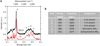 |
Fig. 32 Comparison of aloof EELS and FTIR in the infra-red region on anhydrous guanine crystal (a), EELS : the probe is positioned 30 nm off the guanine edge; FTIR ex situ; (b) : peaks corresponding to C=O, C-H, N-H, NH2 symmetric and NH2 antisymmetric stretches can be seen in the EELS spectrum, matching corresponding features in the FTIR spectrum (from Rez et al. [144]). |
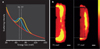 |
Fig. 33 EELS mapping of vibrational excitations in a MgO nanocube of side length 100 nm : (a) spectra produced when the beam is located at a corner (blue), close to a face (yellow), in nearby vacuum (red); (b) maps for energy losses of 70 and 77 meV respectively confirming their corner and face localization (from Lagos et al. [151]). |
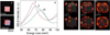 |
Fig. 34 Tomographic surface phonon EELS experiments and reconstruction: (a) HADF images, plane view and tilted view by 400 mrad, of a MgO nanocube of 190 nm edge length; (b) selected spectra recorded at positions indicated in (a) exhibiting maxima fespectively at 68, 69 and 78 meV; (c) 3D vectorial reconstruction of the EMLDOS emphasizing the corner, edge and face localization of the modes I, II and III, the needles indicate the direction of the polarization while the colors indicate the intensity, from red to yellow (courtesy X. Li et al. [153]). |
4 Unconventional present and future domains of application
The development of EELS based techniques over the past sixty years is summarized in terms of accessible performance in space and in energy resolution, in Figure 35. The spatial resolution is directly connected to the minimum size of the specimen to be spectroscopically probed, and its progress in terms of nm−1 is an obvious testimony of the move from micro- to nano-structures and to individual atomic columns or atom-size, nowadays currently accessible thanks to aberration correctors, (E). As for the energy resolution, it governs the quality and accuracy of the information carried in the EELS spectra over a very large spectral domain from the X-ray in the high-energy side to the IR in the low-energy side. In particular, the introduction of monochromators (D) has given access to the exploration of the physics of excitations in extended spectral ranges down to a few meV. When associated on the same microscope column, typical 0.1 nm and 0.1eV on the high energy side or 1 nm and 10 meV on the low energy side are accessible with a high energy electron probe, transforming the STEM-EELS instrument into a spatially resolved “synchrotron beamline” or an “optical bench” (F).
These progresses in instrumentation and methodology have largely broadened the field of application of EELS in the microscope to encompass all types of defects, interfaces, surfaces, nanostructures in solid materials from metals to semiconductors, catalysts and to the frontiers of biomineralization. Furthermore, it has been recently demonstrated that this new generation of spectromicroscopes is also fully dedicated to the exploration of new fields of nanophysics [154]. As an example, the coupling between plasmonic modes in a silver metallic rod and surface phonon vibrations in a supporting thin h-BN layer has been demonstrated by Tizei et al. [155] in a series of experiments performed in situ the electron microscope. The energy value of the plasmonic modes in the nanorod is regularly shifted by successive electron beam milling in order to bring them in resonance with the specific vibrational modes. In these resonance conditions, a strong coupling between the two modes is observed.
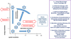 |
Fig. 35 Illustration of the major instrumental progress generating improvements in both spatial and energy resolution in STEM-EELS techniques over the past decades, giving thus access to new domains of research. |
4.1 A multi-dimension acquisition scheme of EELS data
EELS spectrum-imaging has been introduced as a major breakthrough for the acquisition of spatially resolved EELS spectra over an area made of nxm pixels. As illustrated in Figure 7, it consists of a 3D data set built in the (x, y, ΔE) space, and it has been extensively used all along the description of the information carried in the different accessible energy ranges in the previous chapter.
However, this direct relationship between spatial pixels distributed over the surface of the analyzed area and energy channels distributed over a spectral domain, is not the only way of creating 3D data sets. A few examples, shortly mentioned in the above text, have shown that equivalent studies can be realized in the reciprocal, or momentum, space (qx, qy, ΔE). In general, the momentum transfer dependence of vibration modes in crystals has been investigated over decades by bulk approaches such as neutron or x-ray scattering. In order to realize such momentum-resolved investigations with nanoscale resolution, it has been shown that in the STEM-EELS, if one tilts the beam arriving on the specimen surface, it translates the diffraction pattern with respect to the EELS collection aperture and one can thus record local maps (at the resolution of the incident probe) of the reciprocal space cross sections [142]. This approach has recently been used to map optical and acoustical phonons across the first Brillouin zone with a spatial resolution down to <20 nm [146].
Another instrumental control of the EELS measurement is the tilt angle of the specimen with respect to the direction of the primary beam. Recording sets of spectrum-images as a tilt series under tilt angles varying for instance from −60 to +60°, followed by a specific data processing for tomographic reconstruction, provides a 3D (x, y, z) map of a given EELS feature, in reality a 4D object (x, y, z, ΔE). Figures 27 and 34 show respectively 3D spatial maps of surface plasmons and surface vibrational modes on a MgO nanocube, clearly identifying corner, edge and face modes. With the new advanced reconstruction schemes developed to map the vectorial information of the electromagnetic density for plasmonic nanoparticles [136], three dimensional, fully vectorial reconstruction of the phononic electromagnetic local density of states have also been produced [153].
4.2 Time-resolved energy-loss spectroscopy
Time-resolved EELS spectroscopy constitutes another essential extension to 4D data space as spatially resolved chrono-spectra (x, y, ΔE, t). In the early days, a sequence of EELS spectra was recorded as a function of time for a given position of the probe and a natural application was to monitor electron irradiation effects in beam sensitive materials such as insulators [156,157]. The time resolution was then mostly controlled by the speed of acquisition of the detector, typically 30 ms with the Orsay VG STEM. Figure 36 shows a sequence of Al L23 edges recorded while drilling a hole with the high energy primary beam of electrons (109e–/nm2/s in a probe of 1 nm in diameter) through an alumina thin foil and confirms the local transformation of Al2O3 into Al.
Another practical advantage of the time resolved acquisition of sequences of EELS spectra has been used to improve their energy resolution often limited by the instabilities in the high voltage and in the power supplies of the electron optics components. To pass over these limitations, a cheap technique consists in the recording of a 4D SPIM, in which for each pixel, many spectra, typically fifty, are acquired with an acquisition time of a few ms and then summed after re-alignment. It significantly reduces the broadening of the spectra induced by all instrumental instabilities and therefore constitutes an essential step before application of deconvolution techniques [158].
The major progress in time resolution EELS has been introduced by Zewail and coworkers at Cal Tech in the early 2000s with their realization and development of ultrafast electron microscopy (UEM), see [159,160] for reviews. Timed single-electron packets produced by the impact of laser pulses on the electron source of the microscope can overlap with the evanescent electromagnetic field generated by an intense femtosecond pulse of light around a nanostructure, as illustrated in Figure 29b. Practically, in an UEM, the laser fs pulses of a given wavelength are split into two arms, one of them is used to excite a nanostructure (carbon nanotube, silver nanowire), and the other one is used to generate the electron packets at the photocathode electron source of the microscope. The fs timing between the two pulses is controlled by an optical delay line. The synchronization between the electron and photon beams thus generates new spectroscopies as shown in Figure 37, giving access to the study of dynamics states and to energy-loss as well as energy-gain spectra.
As shown in Figure 37d, an energy analysis of the transmitted electron beam having intersected the EM fields generated by the resonant charge oscillations induced on the nanostructure by the incoming laser beam, exhibits a non-Poissonian distribution of peaks incremented with the characteristic energy of the photons, as well in gains as in losses. The origin of these multiphoton absorption and emission effects by the high energy electrons has been theoretically described by Garcia de Abajo et al. [162,163]. As already mentioned above, this PINEM (Photon Induced Near-field Electron Microscopy) technique affords the possibility of directly imaging, in space and time, localized fields at interfaces and “nanoplasmonics” situations [131,164].
Along these directions, Pomarico et al. [165] have reported series of energy filtered images recorded as a function of the photo-exciting laser wavelength. They demonstrate that an energy resolution only limited by the laser linewidth can be reached. This technique constitutes another aspect of multidimensional (4D) spectrum imaging providing space-time-energy resolved frames with meV-fs-nm energy-time-space resolution.
As a matter of fact, the PINEM experiments involve the nanostructure as the necessary intermediate to transfer energy and momentum between the incident high energy free electrons and the photons delivered by the laser, which is impossible in vacuum. But this type of interaction is not informative about the nanostructure by itself. A step forward is made by using a laser wavelength which coincides with a resonant mode of the object. A first success along this direction has been described by Piazza et al. [166]. In their setup, the IR wavelength of the laser pulses coincides with the energy of a specific SP mode on the irradiated silver nanorod, and energy gain maps for this specific energy display the spatial distribution of the SP mode.
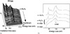 |
Fig. 36 Evolution of the EELS fine structure on the Al L23 edge when drilling a hole in a grain of non-carbon coated α-Al2O3 thin foil : (a) raw chrono-spectral sequence demonstrating the evolution of the edge during the reduction of alumina into aluminum; b) selection of spectra from the previous time-dependent sequence pointing out changes at the edge and above the edge (from Bouchet and Colliex [157]). |
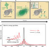 |
Fig. 37 Basic generation of PINEM signals : (a) at t < 0, the electron wave packet of the microscope arrives at the object, a carbon nanotube, before the femtosecond laser pulse and no spatio-temporal overlap occurs between the different fields; (b) at t = 0, the overlap is maximum between photon EM field, the electron wave packet and the evanescent optical field generated by the optical field; (c) at t = 0 or immediately positive, the interaction is maximum and the electron can gain or lose energies equal to integer numbers of the fs laser photon energies; (d) electron energy spectra recorded at two different delay times between the electron and photon beam on the carbon nanotube: for t < 0, only an energy loss spectrum with a single weak peak around 7 eV is visible. But for t = 0, the spectrum exhibits multiple quanta of energy corresponding to the absorption or emission of photons as illustrated in the inset of (c), (from Barwick et al. [161]). |
4.3 From energy-loss (EELS) to energy-gain (EEGS) spectroscopy
These recent experiments in which electrons can increase their energy through the absorption of photons brought by lasers have significantly reboosted old works demonstrating energy gain processes. In their study of EELS of 25 keV across LiF thin foils [138] in the sixties, Boersch et al. had recorded with their high energy resolution instrument [3], energy gain peaks around 50 meV, due to the occurrence of surface ionic vibrations which further disappear when cooling down the specimen to the temperature of liquid air. Another historic experiment by Schilling and Raether [167] had shown the detection of energy gain processes attributed to the interaction of the incoming electron with plasmons already present in the electron gas at the surface of liquid indium. However, these two experiments had been performed without any significant spatial resolution below the micrometer.
With the availability of modern instruments, capable of high spatial- and spectral-energy resolution, respectively below 1 Å and 10 meV, it is not surprising that the temperature dependence of energy gain and energy losses through the interaction of the electron beam with phonons, has been revisited with great care focusing on the detailed behavior of the intensity and energy shift of the associated spectral features. Idrobo et al. [168] study on h-BN nanoflakes the nominal temperature dependence over an energy range between typically 400 and 1000 K, of the Igain/Iloss associated to an optical phonon mode at 186.5 meV and of its energy position and width. Based on the principle of detailed balancing between the gain and loss scattering, Lagos and Batson [169] extract accurate temperature estimates from the measurements and interpretation of the loss and gain P(ΔE)/P(–ΔE) intensity ratios. When they scan the atom-wide monochromatic electron beam over the investigated nanostructure, very refined temperature maps are produced. Exploring transmission and aloof configurations through MgO nanocubes, they verify that this approach applies as well to impact scattering producing vibrational signals modulated by the atomic columns as to dipole scattering at large impact parameters.
As demonstrated in the recent PINEM type experiments, distributions of EEGS peaks using overlapping electron and photon waves around a nanostructure can be mapped. As the development of high brightness pulse electron source is a specialized task and requires a heavy change of instrumentation, alternative solutions have been explored. One of them relying on a pulsed detection system, rather than on a pulse excitation scheme, has been run with success [170].
This has recently been demonstrated with the pulsed-detection sEELS/sEEGS setup tested in Orsay where the STEM is fitted with a light injection on the sample device and with a modified EELS spectrometer and detector (Fig. 38a).
A synchronization electronics allows to adjust the time delay between the laser and deflector pulses so that only the electrons which have interacted with the sample under light irradiation are detected. With this set-up spectral imaging can be performed for the different detected energy losses or gains. An example is shown (Fig. 38b) demonstrating the sensitivity of the technique when optimizing the triggering of the pulse detection with respect to the laser illumination pulse varying the laser around a resonance wavelength. Clear changes of the images of silver nanocubes have also been observed very recently while varying the wavelength of the laser (600nm) with 15 nm changes [171].
These recent developments in technology around STEM-EELS and STEM-EEGS bringing both spatial and spectral resolution, through monochromators and laser injection, to unprecedented levels open fully unexplored fields of research in the ultimate analysis of excited states in the domain of nanophotonics and its applications.
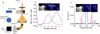 |
Fig. 38 (a): Experimental set-up for the study of laser stimulated EELS and EEGS using a fast detection scheme; (b): EELS spectral-imaging with 900 ms ON time. In this configuration, the sample is illuminated, but most of the detected electrons do not undergo any sEELS/sEEGS event. Inset: HAADF image of the structure (coloured squares indicate the position of the beam where the colour-coordinated spectra in the main panel have been acquired) and filtered images for two main modes. (c): sEELS/sEEGS spectral-imaging with shorter ON time. Specifically, the ON time is close to the laser pulse duration, leading to a clear observation of sEELS/sEEGS features. Inset: HAADF image of the structure (coloured squares indicate the position of the beam where the colour-coordinated spectra in the main panel have been acquired) and filtered images around the energies of the sEELS/sEEGS first peak (courtesy Y. Auad et al. [171]). |
4.4 Multisignal acquisition
As perfectly illustrated in the textbook by Willliams and Carter [172], the EELS signal is only one out of several signals induced by the interaction of the ionizing high velocity primary electrons with the specimen prepared as a thin layer.
Figure 39 shows the different signals generated during such an interaction: a few of them are carried on the directly transferred beam using different sets of detectors, such as an annular dark field one collecting the electrons elastically scattered at large angles and providing HADF images, and a combination of spectrometer and detector for the collection of inelastically electrons and providing the EELS spectra and maps, abundantly described above. Both of them deal with primary events. But through these inelastic scattering processes, energy has been deposited in the specimen and it can be released through different de-excitation mechanisms such as those indicated in the figure. Some can lose the local information but a couple of them measuring the wavelength of the emitted photons constitute very useful secondary events and, depending of their wavelength, they generate X-ray emission signals or Cathodoluminescence (CL) signals, recorded by adapted spectroscopy-detection sets. A clear message resulting from this simple description is that it is most important to collect the most of these generated signals for each incoming high energy electron. This is the basics of the STEM multi-signal approach, which offers learning most information from the studied nano-object [173].
Figure 40 represents the global design of a present STEM optimized for multi-signal acquisition. The emission of photons is carried out by two different acquisition routes depending on the concerned wavelength.
The emission of X rays is analyzed by an EDX detector, in the spectral range of 100 to a few keV. It is then quite complementary to the EELS analysis of core-loss signal and gives direct access to elemental identification with atomic resolution thanks to the implementation of X-ray detectors with much enhanced collection efficiency [174,175]. As a demonstration of the ultimate sensitivity of the association of these two techniques (core-loss EELS and EDX), Suenaga et al. have shown characteristic EDX signals (Er M and Er L) and EELS signals (Er L) from individual doping Er ions in peapods encapsulated in single-walled carbon nanotubes [176].
At the low-energy side of the energy spectrum (from the near IR below 1 eV to the UV), now accessible in EELS thanks to the energy resolution improvement associated with the monochromators, photons in the visible range and around can now be detected and analyzed. This CL technique has demonstrated its efficiency for studying the emission spectrum from individual nanostructures or defects, such as quantum dots, fluorescent ions, molecules and clusters, using a specifically settlement combining optical spectrometry and detection facing directly the specimen [177,178]. A commercially distributed CL device allowing input as well as output of light in a STEM column is now available on the market from Attolight AG (https://attolight.com/). A review of the state of the development and use of CL in the STEM can be found in [179].
When replacing the optical spectrometer on the light output line from the microscope column by an intensity interferometer (generally of Hanbury, Brown and Twiss) HBT type, one can measure the time correlation between the arrival of photons [g(2) (τ)], and have thus access to quantum electrodynamics world and properties: photon antibunching characteristics of single photon emitters [180], photon bunching arising from the synchronization of multiple excitations via primary excitation decay into multiple e-h pairs [181], life-time measurements from quantum emitters separated by only a few nanometers [182].
The useful impact of associating EELS and CL techniques for investigating the field of “nanoplasmonics”, and more generally of nanophotonics, has been largely described above and illustrated in Figures 29 and 30. It can also probe the local emission of light from elementary solid state excitations, such as excitons and trions on nm scale in inhomogneous material. As an example, Figure 41 compares the EELS and the CL spectra recorded on a monolayer of transition metal dichalcogenide (WS2), which is a direct bandgap semiconductor with bright luminescence due to exciton decay.
In a study presently under development at LPS Orsay, N. Bonnet et al. explore with a combination of the two signals on the same sample area, the variation of the light emission from the XA exciton in a monolayer of WS2 encapsulated between h-BN thin layers. The XB exciton detected in the EELS spectrum does not emit light while the negatively charged X– trion (separated from the XA exciton by 35 meV and not resolved in the EELS spectrum) exhibits nanoscale inhomogeneous variations of light emission the origin of which is under search [183]. For sure, with these new openings in spectroscopy instrumentation and methods delivering the largest panel of signals, innovative fields of research will be opened in condensed matter physics as well as in nanophotonics at the ultimate spatial resolution.
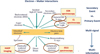 |
Fig. 39 Different signals generated during the interaction of the incident high-kV electron beam and the thin specimen (reproduced from [170, page 7]). |
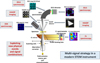 |
Fig. 40 Illustration of a multi-signal acquisition scheme on a most recent STEM instrument, delivering simultaneously an HADF image, an EELS signal, an emitted EDX photon image with atomic resolution, and a visible light type image with nm resolution. |
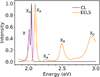 |
Fig. 41 Emission and absorption of a WS2 monolayer measured by CL and EELS on the same specimen area with the STEM Chromatem at LPS Orsay (courtesy N. Bonnet et al. [183]). |
4.5 Towards a “nanolaboratory”
The whole field of transmission electron microscopy is in rapid evolution and a most important one is the development of dedicated specimen stages accommodating the imaging, diffraction and spectroscopies of specimens under external solicitations. This is a very old requirement [184] and tilting stages, variable temperature stages, variable pressure stages, liquid stages and stages incorporating external mechanical, or electric fields or in situ irradiation sources or light illumination, have been continuously designed, elaborated and used over the past decades. This trend has fully benefited from the enlarged gap space between the objective pole pieces in Cs corrected microscopes, to host the light injectors, the nano-indentation systems or the environmental cells required for realizing in situ measurements while keeping a permanent eye on what is happening at the ultimate spatial resolution. One can nowadays consider that many recent TEM columns have been upgraded into “nanolaboratories” where dedicated experiments can be performed on nanostructures. In particular, the richness of the information delivered by EELS measurements and the associated multisignal exploitation is and will undoubtedly be exploited in situ in the TEM column.
As a first example, EELS measurements have been realized over a large temperature range, from liquid helium up to 1000 °C and above, and have efficiently contributed to the study of the electron excitations in nanosized areas and in particular to their changes during temperature variation. Over fifty years ago, we built a liquid helium stage [185] which provided spectral information from the band gaps to the collective excitations in crystallites of solidified rare gases [83]. Very recently, the information carried by the shift of the volume plasmon peak in metallic Al [97] or by the combination of the gain and loss peaks in the optical phonon excitation mode in h-BN [169] has been used for nanoscale temperature measurements over moderate (318 to 419 K in [97]) or extended (320 to 1600 K in [169]) temperature ranges.
As a demonstration of the interest of recording EELS spectra while ramping the temperature of a specimen over a range, Figure 42 shows series of low-loss excitations in the IR spectral domain associated to electronic (metal M/insulator I) transitions in V2O3 [186]. When cooled below 160K, it is known that V2O3 undergoes both a structural and an electronic transition from metallic to insulating state accompanied with a resistivity variation of 7 orders of magnitude. Using the Chromatem at Orsay, equipped with the double-tilt HennyZ cyoholder combined with MEMS for heating up locally the specimen (see Fig. 42a), the EELS spectra display a characteristic plasmonic feature at 1.1 eV only in the metallic phase: it disappears between 138 and 141 K when cooling (Fig. 42b) and appears between 149 and 153 when heating (Fig. 42c). In the intermediate temperatures, the coexistence of nanoscale domains could be evidenced. This example clearly demonstrates the great potential impact of variable temperature EELS measurements for solving basic condensed nano-materials issues.
Another spectacular technological development opening a large panel of new research domains is that of liquid cells for imaging and analyzing hydrated samples and water itself, but also for monitoring the dynamics of chemical and electronic processes around and on the surfaces of nanoparticles in liquids. In the textbook on Liquid Cell Electron Microscopy edited in 2017 by Frances Ross [188], one can find general information [189] as well as a chapter on the design and fabrication of encapsulated liquid cells. They use microfabricated chip designs based on SiN material [190] or graphene layers as the windows material enable to trap small pockets of liquids containing the nano-objects of interest [191]. EELS studies are generally limited by cell thickness but graphene liquid cells offer substantial possibilities of elemental mapping and of probing liquid phase reactions at nanometer-resolution in spite of their increased beam damage susceptibility, see [192,193].
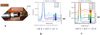 |
Fig. 42 EELS spectromicroscopy under variable temperature on a V2O3 specimen: (a) cryo-double-tilt side entry in situ HennyZ holder cooled at LN2 [187]; (b) series of low-loss excitations recorded upon cooling and (c) under heating, displaying the detection of a plasmonic feature at 1.1 eV in the metallic state [186]. |
4.6 Using a shaped-electron beam for EELS measurements
The characteristics of the primary electron beam, such as its high voltage and energy width (with or without monochromator) constitute key parameters for defining the field of applications of the attached EELS spectrometer. However, when compared to a photon beam, the (S)TEM electron beam, as it is, lacks from a polarization control. Therefore, over the past years, many efforts have been devoted to prepare a free electron into a vortex beam, i.e. a spiraling wavefront carrying an angular momentum around its propagation direction.
A first example has been the development of methods for the analysis and characterization of magnetic materials at the nm scale. EMCD (EELS Magnetic Chiral Dichroism) has been first proposed and demonstrated by Schattschneider et al. [194] using similar principles as in the XMCD (Xray Magnetic Circular Dichroism) in which the absorption cross section of the incident monochromatic X ray beam in a synchrotron changes when the helicity of the circularly polarized photons is reversed. In a TEM, the EMCD is accessible through the inelastic electron scattering under particular conditions. The EELS dichroic magnetic signal is measured as the difference between two L23 spectra recorded on an iron thin foil placed in the strong magnetic field of the microscope objective lens, when the detector aperture is positioned in two symmetric situations (+) and (–) with respect to a strong 2-beam diffraction condition.
The generation of electron beams carrying an angular orbital momentum has then been studied in a more general approach in which a plane wave is converted into a spiral-type wave using a spiral phase plate [195]. In this work, the spiral like phase plate is composed of overlapping graphite thin films and generates an electron beam with a phase singularity of signature l = 1as revealed by electron holography as a ‘Y’-like defect pattern in an interference pattern. Then, Verbeeck et al. [196] have created vortex electron beams, with a phase singularity and carrying an angular momentum around their propagation direction, using an holographic reconstruction technique in a (S)TEM, see Figure 43. Binary masks which either block or pass electrons in specific places are realized with focused ion beam instruments. The associated diffraction pattern encompasses the central beam carrying an angular momentum corresponding to l = 0, and two symmetric satellite spots carrying angular momentum of respectively ±ħ corresponding to l = +1 and l = –1. When used for studying energy loss magnetic circular dichroism on a specimen such as a thin foil of Fe submitted to the external magnetic field of the objective lens of the electron microscope column, an asymmetry is observed in the intensity of the white lines associated to the core excitations of 2pj −> 3d type with j = 1/2 or 3/2 as shown in Figure 43b. The intensity of these transitions is governed by spherical harmonic matrix elements which provide OAM to the inelastically scattered fast electrons.
Another way of shaping the wave function of the primary electron beam to explore the different symmetries of the excitation modes which it creates on nanoparticles, has recently been described by Guzzinati et al. [197]. A two-lobed beam is generated through an aperture in which the two transferred halves are opposite in phase, as for instance with a microscopic ferromagnetic needle of length much larger than the aperture diameter. It has been used with success to map plasmonic excitations on metallic nanorods, with the selective detection of dipolar resonances, similarly to what is generally revealed by linearly polarized light, but with a much enhanced spatial resolution.
In the description of the time-resolved EELS spectroscopy and the PINEM technique (see above [159–161], we have introduced the role of acting on the primary beam of electrons reducing it into timed single-electron packets by focusing a laser fs on the emitting metallic cathode. This achievement has stimulated a more general effort of research on the optical shaping of electron beams based on light-electron interaction processes. Swift electrons travelling through the evanescent light fields created aloof nanostructures can generate multiphoton absorption and emission processes as theoretically proposed in [163] and realized in [198]. In this work, ultra-short electron pulses are interacting with the optical near field of a nanostructure, thus being phase-modulated and exchanging energy, through Rabi oscillations, in integer multiples of the photon energy (see Fig. 44). When implemented on a field emitter tip, these authors have demonstrated record pulse properties in ultrafast electron microscopy with a 9 Å diameter beam, 200 fs pulse duration and 0.6 eV energy width [199]. More recent developments, relying on innovative techniques for modulating the phase control of the electron beam, have been used and tested. A first one relies on the superposition of free electron states generated by nanostructures creating two separated near fields with polarization anisotropy [200]. Recently, the interaction between electron and photon has been significantly enhanced by replacing the acting metallic tip by photonic cavities and whispering gallery modes carried by dielectric micro-resonators. A spectral broadening of the co-propagating electrons in the beam has been realized up to 700 eV, corresponding to the absorption or emission of hundreds of photons [201]. A demonstration of ultra-fast TEM for multi-dimensional spectroscopy (space, momentum, energy polarization and time) has been demonstrated.
These studies open innovative routes for the quantum control of free electrons opening the path to many innovative developments in quantum information processing and quantum sensing [202].
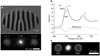 |
Fig. 43 (a) A binary mask in a Pt thin foil generated by ion beam under computer control design, exhibiting a dislocation type geometry, and its diffraction pattern exhibiting two satellite vortex spots carrying opposite l = 1 and l = -1 OAM; (b) EELS spectra of the L3 and L2 lines in a Fe thin foil, recorded with the right and left satellite vortex spots. Their difference in intensity shows the magnetic circular dichroism of the specimen homogeneously magnetized by the magnetic field of the objective lens (from Verbeeck et al. [196].) |
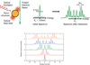 |
Fig. 44 A pulsed electron beam traversing an intense optical near-field exhibits an energy distribution with multiple spectral sidebands, the number of which varying with the optical field strength (from Feist et al. [199]). |
4.7 A few timely conclusions
For sure, the instrumentation for the acquisition of innovative EELS spectra and the theoretical tools for their interpretation have benefited of so many progresses over the past five decades that an update of the previous review published in 1984 and republished in 2019, was urgently required. Beyond the aberration corrected spectrometer which collects larger angular distribution of the inelastic electrons improving the signal-to-noise of the spectra and the monochromator which brings the energy resolution in the 10 meV range, the whole design of the nowadays STEM microscopes in all its components has also benefited from important changes and progress. The aberration corrector has significantly improved the spatial resolution providing access to sub-Å at lower primary voltages. Furthermore, it is generally associated with an enlarged gap in the objective lens offering more space for the acceptance of many special specimen stages, thus giving access to diverse possibilities of heating, cooling, mechanical deformation, in situ gas or liquid environment. It is also well suited to the implementation of photonic devices for the recording of emitted photons (simultaneous CL) or for injecting them: all these additions definitely transform the microscope into a nanolaboratory. The continuous development of direct Si-based quantum electron detectors with their increased dynamic range and ultra-fast acquisition opens new technical applications, such as the real time drift correction (as illustrated in Fig. 6), and new fields of research, such as dynamic studies of highly localized specimen changes. It is therefore an opening to future studies which we can now realize with atomic spatial resolution such as mapping the nature and bonding of atoms, their mass and possibly the isotopes, and also very localized electromagnetic fields or the local temperature !!
Another important consequence is that this development of analytical electron microscope in the STEM generates huge volumes of data. For instance, one spectrum-image (SI) is typically made of 104 up to 106 pixels × 103 energy channels. It is therefore useful to consider it as a full data set and to exploit the redundant nature of information with the help of statistical techniques such as the principal component analysis (PCA) which has been exploited since many years. Recently, spectral unmixing methods of hyperspectral STEM-EELS images have largely been elaborated around the world, and are described in the Hyperspy toolbox [45]. Deep Learning (DL) and Artificial Intelligence (AI) methods are fully operational in this task. What may be the future? In this direction, Spurgeon et al. suggest that these presently elaborated data-driven methods will play a major role in the construction of the next generation transmission electron microscope, related to experiment design, feature extraction towards enlarged knowledge discovery [203].
Table of abbreviations
ADF: Annular Dark Field
HAADF: High Angle Annular Dark Field
MAADF: Medium Angle Annular Dark Field
BF: Bright Field
CCD: Charge Coupled Device
CL: CathodoLuminescence
CMOS: Complementary Metal Oxide Semiconductor
(C)TEM: (Conventional) Transmission Electron Microscope
EFTEM: Energy Filtering Transmission Electron Microscope
DFT: Density Functional Theory
TDDFT: Time Dependent Density Functional Theory
DQE: Detection Quantum Efficiency
EDX: Energy Dispersive X-ray spectroscopy (or Spectrum)
EEGS: Electron Energy Gain Spectroscopy
sEEGS: Stimulated EEGS
EELS: Electron Energy Loss Spectroscopy
sEELS: Stimulated EELS
EMLDOS: Electro Magnetic Local Density Of States
FEG: Field Emission (electron) Gun
LSP: Localized Surface Plasmon
SPP: Surface Plasmon Polariton
MLLS: Multiple Linear Least Square
MO: Molecular Orbital
PCA: Principal Component Analysis
ICA: Independent Component Analysis
PINEM: Photon Induced Near-field Electron Microscopy
Pl: Plasmon
IPl: Interface Plasmon
Q: Quality Factor = ratio of absolute energy and width of a spectral line
SI (or SPIM): Spectrum Image (or Spectrum Imaging)
SNR: Signal to Noise Ratio
(S)TEM: (Scanning) Transmission Electron Microscope
UEM: Ultrafast Electron Microscope
VEELS: Valence Electron Energy Loss Spectroscopy
ZLP: Zero Loss Peak
Acknowledgements
This review relies on studies realized over more than four decades in the Orsay STEM group at the Laboratoire de Physique des Solides. Consequently, many Ph.D. students, post-docs, visitors, technicians, engineers, permanent researchers and long-term collaborators have been involved in the developments in instrumentation, in data acquisition and processing, in theoretical simulations, in the welcome of external visitors for running experiments on many different topics requiring top level machines.
A Vacuum Generators HB05 dedicated STEM, was acquired in 1980 and first tested by Claudie Mory and Paul Ballongue, and the parallel EELS spectrometer developed by Ondrej Krivanek was first installed a few years later. The spectrum-image acquisition mode proposed by Christian Jeanguillaume and installed by Marcel Tencé provided in the mid 90s unique results on complex nanotubes by Odile Stéphan and Mathieu Kociak in collaboration with Pulickel Ajayan and Kazutomo Suenaga, up to the identification of single atoms in the year 2000. It was followed by a rich period of solving different issues in condensed matter physics by Alexandre Gloter, Tahar Manoubi, Mike Walls, Raul Arenal, Laura Bocher or testing these tools in new domains such as biochemistry by Marta de Frutos. In parallel, the revival of plasmon studies under the leading role of Odile Stéphan and Mathieu Kociak with a younger generation (Daniel Ugarte, Dario Taverna, Stefano Mazzucco, Jaysen Nelayah, Arthur Losquin) was followed by the international blossoming of plasmonics accompanied by the simultaneous development of cathodoluminescence (CL) measurements (Luiz Zagonel, Luiz Tizei, Sophie Meuret). This unique microscope, under the permanent supervision of Marcel Tencé and his attention to regularly update it with new attachments and adapted pieces of software, is still in operation in 2020 daily delivering new results mostly in low temperature CL.
Relying on the experience gathered with this first STEM, the team has acquired successively in 2011 and 2018 two microscopes of the latest generation: a NION UltraStem microscope equipped with an aberration corrector bringing the probe size down to the angström level, a NION Chromatem microscope equipped with both aberration corrector and monochromator opening the access to measurements simultaneously in the Å and the 10 meV energy range and the associated exploration of the phonon world. The chapters dealing with the low energy excitations as well as with the unconventional present and future domains of applications are directly issued from the remarkable work performed by the young generation of engineers of the team, around Marcel Tencé, with Jean-Denis Blazit, Katia March, Xiaoyan Li, together with new Ph.Ds and post docs Almudena Torres-Pardo, Marina Marinova, Pabitra Das, Romain Bourrelier, Steffi Woo, Guillaume Boudarham, Hugo Lourenço-Martins, Yves Auad, Anna Tararan, Alfredo Campos, Adrien Teurtrie, Noémie Bonnet a few of them having directly contributed to this manuscript with their figures illustrating the text. Another consequence of the results obtained with the microscopes is that they are so many and diversified that they deserve the support of new tools in data processing, which are elaborated and tested in particular by Nathalie Brun, and theoretical simulations by Alberto Zobelli, and Michele Amato.
All my warmest thanks to all of them for their presence around me, in particular to Odile Stéphan who has beautifully led the group over the past twelve years since my retirement.
References
- J. Hillier, R.F. Baker, Microanalysis by means of electrons, J. Appl. Phys. 15, 663 (1944) [CrossRef] [Google Scholar]
- G. Ruthemann, Diskrete Energie verluste mittelschneller Elektronen beim Durchgang durch dünne Folien, Ann. Phys. 6, 113 (1948) [CrossRef] [Google Scholar]
- H. Boersch, J. Geiger, H. Hellwig, Steigerung der Auflösung bei der Elektronen-Energieanalyse, Phys. Lett. 3, 64 (1962) [CrossRef] [Google Scholar]
- R. Castaing, L. Henry, Filtrage magnétique des vitesses en microscopie électronique, C. R. Acad. Sci. Paris 255, 76 (1962) [Google Scholar]
- D.B. Wittry, R.P. Ferrier, V.E. Cosslett, Selected-area spectrometry in the transmission electron microscope, Br. J. Appl. Phys. D 2, 1767 (1969) [CrossRef] [Google Scholar]
- D.B. Wittry, An electron spectrometer for use in the transmission electron microscope, Br. J. Appl. Phys. D 2, 1757 (1969) [CrossRef] [Google Scholar]
- M. Isaacson, Interaction of 25 keV electrons with the nucleic acid bases, adenine, thymine and uracil. I. Outer shell electrons, J. Chem. Phys. 56, 1803 (1972) [CrossRef] [Google Scholar]
- M. Isaacson, Interaction of 25 keV electrons with the nucleic acid bases, adenine, thymine and uracil. II. Inner shell excitation and inelastic scattering cross section, J. Chem. Phys. 56, 1813 (1972) [CrossRef] [Google Scholar]
- A.V. Crewe, M. Isaacson, D. Johnson, A high resolution electron spectrometer for use in transmission scanning electron microscopy, Rev. Sci. Instrum. 42, 411 (1971) [CrossRef] [PubMed] [Google Scholar]
- C. Colliex, B. Jouffrey, Contribution à l’étude des pertes d’énergie dues à l’excitation de niveaux profonds, C. R. Acad. Sci. Paris B 270, 144 (1970) [Google Scholar]
- C. Colliex, B. Jouffrey, Images filtrées obtenues avec des électrons ayant subi des pertes d’énergie dues à l’excitation de niveaux profonds, C. R. Acad. Sci. Paris B 270, 673 (1970) [Google Scholar]
- C. Colliex, B. Jouffrey, Diffusion inélastique des électrons dans un solide par excitation de niveaux atomiques profonds. I - Spectres de pertes d’énergie, Philos. Mag. 25, 491 (1972) [CrossRef] [Google Scholar]
- R.F. Egerton, Inelastic scattering and energy filtering in the transmission electron microscope, Philos. Mag. 34, 49 (1976) [CrossRef] [Google Scholar]
- R.F. Egerton, Formulae for light-element microanalysis by electron energy-loss spectrometry, Ultramicroscopy 3, 243 (1978) [CrossRef] [PubMed] [Google Scholar]
- M. Isaacson, D. Johnson, The microanalysis of light elements using transmitted energy-loss electrons, Ultramicroscopy 1, 33 (1975) [CrossRef] [PubMed] [Google Scholar]
- C. Colliex, V.E. Cosslett, R.D. Leapman, P. Trebbia, Contribution of energy-loss spectroscopy to the development of analytical electron microscopy, Ultramicroscopy 1, 301 (1976) [CrossRef] [PubMed] [Google Scholar]
- M.S. Isaacson, J. Silcox, Report of a workshop on analytical electron microscopy, Cornell U. August 1976, Ultramicroscopy 2, 89 (1976) [CrossRef] [PubMed] [Google Scholar]
- C. Colliex, Electron energy loss spectroscopy in the electron microscope, in Advances in Optical and Electron Microscopy, edited by R. Barer and V.E. Cosslett (1984), Vol. 9,pp. 65–177, [reprinted in Adv. Imag. Electr. Phys. 211, 187(2019)] [Google Scholar]
- O.L. Krivanek et al., Vibrational spectroscopy in the electron microscope, Nature 514, 209 (2014) [CrossRef] [PubMed] [Google Scholar]
- O.L. Krivanek, T.C. Lovejoy, N. Dellby, R.W. Carpenter, Monochromated STEM with a 30-meV wide, atom-sized electron probe, Microscopy 62, 3 (2013) [CrossRef] [PubMed] [Google Scholar]
- A.V. Crewe, M. Isaacson, D. Johnson, A simple scanning electron microscope, Rev. Sci. Instrum. 40, 241 (1969) [CrossRef] [Google Scholar]
- A.V. Crewe, J. Wall, J. Langmore, Visibility of single atoms, Science 168, 1338 (1970) [CrossRef] [PubMed] [Google Scholar]
- K. Suenaga et al., Element-selective single atom imaging, Science 290, 2280 (2000) [CrossRef] [PubMed] [Google Scholar]
- M. Haider et al., Electron microscopy image enhanced, Nature 392, 768 (1998) [CrossRef] [Google Scholar]
- O.L. Krivanek, N. Dellby, A.R. Lupini, Towards sub-å electron beams, Ultramicroscopy 78, 1 (1999) [CrossRef] [Google Scholar]
- K. Kimoto et al., Element-selective imaging of atomic columns in a crystal using STEM and EELS, Nature 450, 702 (2007) [CrossRef] [PubMed] [Google Scholar]
- M. Bosman et al., Two-dimensional mapping of chemical information at atomic resolution, Phys. Rev. Lett. 99, 086102 (2007) [CrossRef] [PubMed] [Google Scholar]
- D.A. Muller et al., Atomic-scale chemical imaging of composition and bonding by aberration-corrected microscopy, Science 319, 1073 (2008) [CrossRef] [PubMed] [Google Scholar]
- See for a review: P.W. Hawkes, O.L. Krivanek, in Springer Handbook of Microscopy, edited by P.W. Hawkes, J.C.H. Spence (Springer, 2020) https://doi.org/10.1007/978-3-030-00069-1_13; [Google Scholar]
- See for a review K. Kimoto, Practical aspects of electron monochromators developed for transmission electron microscopy, Microscopy 63, 337 (2014) [CrossRef] [PubMed] [Google Scholar]
- H. Shuman, Parallel recording of electron energy-loss spectra, Ultramicroscopy 6, 163 (1981) [CrossRef] [PubMed] [Google Scholar]
- H. Shuman, P. Kruit, Quantitative data processing of parallel recorded electron energy-loss spectra with low signal to background, Rev. Sci. Instrum. 56, 231 (1985) [CrossRef] [Google Scholar]
- O.L. Krivanek, C.C. Ahn, R.B. Keeney, Parallel detection electron spectrometer using quadrupole lens, Ultramicroscopy 22, 103 (1987) [CrossRef] [Google Scholar]
- J. Scott et al., Near-simultaneous dual energy range EELS spectrum imaging, Ultramicroscopy 108, 1586 (2008) [CrossRef] [PubMed] [Google Scholar]
- M. Tencé et al., A new detector device designed for quantitative EELS spectroscopy, Proc. IMC 16 (2006), Sapporo, Japan edited by H. Ichinose; T. Sasaki (2006), pp. 824–825 [Google Scholar]
- K. March et al., in Addressing challenges in electron energy-loss spectroscopy on individual atoms, Proc. IMC 18 (2014), Prague, Czech. Republic, edited by P. Hozak (2014) IT-5-P-6028 [Google Scholar]
- G. McMullan, A.R. Faruqui, D. Clare, R. Henderson, Comparison of optimal performance at 300 keV of three direct electron detectors for use in low dose electron microscopy, Ultramicroscopy 147, 156 (2014) [CrossRef] [PubMed] [Google Scholar]
- J.L. Hart et al., Direct detection electron energy loss spectroscopy : a method to push the limits of resolution and sensitivity, Sci. Rep. 7, 8243 (2017) [CrossRef] [Google Scholar]
- The Nobel Prize in Chemistry 2017 is awarded to Jacques Dubochet, Joachim Frank and Richard Henderson for “developing cryo-electron microscopy for the high-resolution structure determination of biomolecules in solution”, https://www.nobelprize.org/uploads/2018/06/press-41 [Google Scholar]
- J.A. Mir et al., Characterisation of the Medipix3 detector for 60 and 80 keV electrons, Ultramicroscopy 182, 44 (2017) [CrossRef] [PubMed] [Google Scholar]
- R. Castaing, L. Henry, Filtrage magnétique des vitesses en microscopie électronique, C.R. Acad. Sci. Sér. B 255, 76 (1962) [Google Scholar]
- C. Jeanguillaume, C. Colliex, Spectrum-image: the next step in EELS digital acquisition and processing, Ultramicroscopy 28, 252 (1989) [CrossRef] [Google Scholar]
- J.A. Hunt, D. Williams, Electron energy-loss spectrum imaging, Ultramicroscopy 38, 47 (1991) [CrossRef] [Google Scholar]
- J.L. Lavergne, J.M. Martin, L. Belin, Interactive electron energy-loss elemental mapping by the Imaging-Spectrum method, Microsc. MicroanaL Microstruct. 3, 517 (1992) [CrossRef] [EDP Sciences] [Google Scholar]
- HyperSpy: multi-dimensional data analysis toolbox – https://hyperspy.org/index.html [Google Scholar]
- S. Lichtert, J. Verbeeck, Statistical consequences of applying a PCA noise filter on EELS spectrum images, Ultramicroscopy 125, 35 (2013) [CrossRef] [PubMed] [Google Scholar]
- J. Spiegelberg, J. Rusz, K. Pelckmans, Tensor decompositions for the analysis of atomic resolution electron energy loss spectra, Ultramicroscopy 175, 36 (2017) [CrossRef] [PubMed] [Google Scholar]
- F. de la Peňa et al., Mapping titanium and zinc oxide phases using EELS: an application of Independent Component Analysis, Ultramicroscopy 111, 169 (2011) [CrossRef] [PubMed] [Google Scholar]
- N. Bonnet, D. Nuzillard, Independent Component Analysis: a new possibility for analyzing series of electron energy loss spectra, Ultramicroscopy 102, 327 (2005) [CrossRef] [PubMed] [Google Scholar]
- J.M.P. Nascimento, J.M.B. Dias, Vertex Component Analysis: a fast algorithm to unmix hyperspectral data, IEEE Trans. Geosci. Remote Sens. 43, 898 (2005) [CrossRef] [Google Scholar]
- N. Dobigeon et al., Joint bayesan endmember extraction and linear unmixing for hyperspectral imagery, IEEE Trans. Signal Process. 57, 4355 (2009) [CrossRef] [MathSciNet] [Google Scholar]
- N. Dobigeon, N. Brun, Spectral mixture analysis of EELS spectrum-images, Ultramicroscopy 120, 25 (2012) [CrossRef] [PubMed] [Google Scholar]
- A. Zobelli et al., Dynamic random scan approach of spectrum imaging for temporal evolution of spectroscopic signals, Microsc. Microanal. 25, 162 (2019) [CrossRef] [Google Scholar]
- E. Monier et al., Reconstruction of partially sampled multiband images — application to STEM-EELS imaging, IEEE Trans. Comput. Imag. 4, 585 (2018) [CrossRef] [Google Scholar]
- A. Zobelli et al., Spatial ad spectral dynamics in STEM hyperspectral imaging using random scan patterns, Ultramicroscopy 212, 112912 (2020) [CrossRef] [PubMed] [Google Scholar]
- R.F. Egerton, Electron energy-loss spectroscopy in the electron microscope, 1st edn. (Plenum Press, 1986), 2nd edn., (Plenum Press, 1996) 3rd edn. (Springer, 2011) [Google Scholar]
- R.F. Egerton, Formulae for light element analysis by electron energy loss spectrometry, Ultramicroscopy 3, 243 (1978) [CrossRef] [PubMed] [Google Scholar]
- R.F. Egerton, K-shell ionization cross-sections for use in microanalysis, Ultramicroscopy 4, 169 (1979) [CrossRef] [Google Scholar]
- R.D. Leapman, P. Rez, D.F. Mayers, K, L and M shell generalized oscillator strengths and ionization cross sections for fast electron cross sections, J. Chem. Phys. 72, 1232 (1980) [CrossRef] [Google Scholar]
- J. Verbeeck, S. Van Aert, G. Bertoni, Model-based quantification of EELS spectra: including the fine structure, Ultramicroscopy 106, 976 (2006) [CrossRef] [PubMed] [Google Scholar]
- R. Arenal et al., Extending the analysis of EELS spectrum-imaging data, from elemental to bond mapping in complex nanostructures, Ultramicroscopy 109, 32 (2008) [CrossRef] [PubMed] [Google Scholar]
- K. Kimoto et al., Element-selective imaging of atomic columns in a crystal using STEM and EELS, Nature 450, 702 (2007) [CrossRef] [PubMed] [Google Scholar]
- M. Bosman et al., Two-dimensional mapping of chemical information at atomic resolution, Phys. Rev. Lett. 99, 086102 (2007) [CrossRef] [PubMed] [Google Scholar]
- D.A. Muller et al., Atomic-scale chemical imaging of composition and bonding by aberration-corrected microscopy, Science 319, 1073 (2008) [CrossRef] [PubMed] [Google Scholar]
- A. Gloter et al., Atomically resolved mapping of EELS fine structures, Mater. Sci. Semicond. Process 65, 2 (2017) [CrossRef] [Google Scholar]
- J.A. Tossell, D.J. Vaughan, K.H. Johnson, The electronic structure of rutile, wustite and hematite from molecular calculations, Am. Mineral. 59, 319 (1974) [Google Scholar]
- C. Colliex, T. Manoubi, C. Ortiz, Electron energy-loss spectroscopy near-edge fine structures in the iron oxygen system, Phys. Rev. B 44, 402 (1991) [Google Scholar]
- S.-Y. Chen et al., Electron energy loss spectroscopy and ab initio investigation of iron oxide nanomaterials grown by a hydrothermal process, Phys. Rev. B 79, 104103 (2009) [CrossRef] [Google Scholar]
- G. Radtke, G.A. Botton, in Energy loss near-edge structures, Scanning Transmission Electron Microscopy, edited by S.J. Pennycook, P.D. Nellist (Springer Science+Business Media, 2011), pp. 207–245 [Google Scholar]
- A. Torres-Pardo et al., Spectroscopic mapping of local structural distorsions in ferroelectric PbTi03/SrTiO3 superlattices at the unit-cell scale, Phys. Rev. B 84, 220102(R) (2011) [CrossRef] [Google Scholar]
- K. Suenaga et al., Visualizing and identifying single atoms using electron energy-loss spectroscopy with low accelerating voltage, Nat. Chem. 1, 415 (2009) [CrossRef] [PubMed] [Google Scholar]
- H. Tan et al., 2D atomic mapping of oxidation states in transition metal oxides by scanning transmission electron microscopy and electron energy loss spectroscopy, Phys. Rev. Lett. 107, 107602 (2011) [CrossRef] [PubMed] [Google Scholar]
- L. Bocher et al., Direct evidence of Fe2+ - Fe3+ charge ordering in the ferrimagnetic hematite -ilmenite Fe1.35Ti0.65O3-d thin film, Phys. Rev. Lett. 111, 167202 (2013) [CrossRef] [PubMed] [Google Scholar]
- S. Turner et al., Site-specific mapping of transition metal oxygen coordination in complex oxides, Appl. Phys. Lett. 101, 241910 (2012) [CrossRef] [Google Scholar]
- H. Raether, Electron energy loss spectroscopy, Springer Tracts, Mod. Phys. 38, 85 (1965) [Google Scholar]
- J. Daniels et al., Optical constants of solids by electron spectroscopy, in Springer Tracts Mod. Phys. (Springer Verlag, New York, 1970) Vol. 54, pp. 78–135 [Google Scholar]
- H. Raether, Excitation of plasmons and interband transitions by electrons, in Springer Tracts Mod. Phys. (Springer, Berlin, 1980), Vol. 88 [Google Scholar]
- C. Colliex, Electron energy-loss spectroscopy on solids, in International tables of Crystallography, Chapter 4-3-3d (1992), pp. 338–359 [Google Scholar]
- M. Couillard et al., Multiple-interface coupling effects in local electron energy-loss measurements of band gap energies, Phys. Rev. B 76, 165131 (2007) [CrossRef] [Google Scholar]
- L. Hung et al., Interpretation of monoclinic hafnia valence electron energy-loss spectra by time-dependent density functional theory, Phys. Rev. B 93, 165105 (2016) [CrossRef] [Google Scholar]
- N. Vast et al., Local field effects in the electron energy loss spectra of rutile Ti O2, Phys. Rev. Lett. 88, 037601 (2002) [CrossRef] [PubMed] [Google Scholar]
- L.K. Dash et al., Electronic structure and electron energy-loss spectroscopy of ZrO2 zirconia, Phys. Rev. B 70, 245116 (2004) [CrossRef] [Google Scholar]
- C. Colliex, B. Jouffrey, Pertes d’énergie dans des couches minces de gaz solidifiés, J. Phys. 32, 461 (1971) [CrossRef] [EDP Sciences] [Google Scholar]
- R. Haensel et al., Reflection spectrum of solid argon in the vacuum ultra-violet, Phys. Rev. Lett. 23, 1160 (1969) [CrossRef] [Google Scholar]
- U. Rössler, Electron and exciton states in solid rare gases, Phys. Status Solidi 42, 345 (1970) [CrossRef] [Google Scholar]
- S. Schamm, G. Zanchi, Study of the dielectric properties near the band-gap by VEELS: gap measurements in bulk materials, Ultramicroscopy 96, 559 (2003) [CrossRef] [PubMed] [Google Scholar]
- B. Rafferty, L.M. Brown, Direct and indirect transitions in the region of the band-gap investigated by electron energy-loss spectroscopy, Phys. Rev. B 58, 10326 (1998) [CrossRef] [Google Scholar]
- P. Moreau, M.C. Cheynet, Improved comparison of low energy-loss spectra with band structure calculations: the example of BN filaments, Ultramicroscopy 94, 293 (2003) [CrossRef] [PubMed] [Google Scholar]
- S. Lazar et al., Materials science applications of HREELS in near-edge structure analysis and low energy loss spectroscopy, Ultramicroscopy 96, 535 (2003) [CrossRef] [PubMed] [Google Scholar]
- R. Erni, N.D. Browning, Valence electron energy-loss spectroscopy in monochromated scanning transmission electron microscopy, Ultramicroscopy 104, 176 (2005) [CrossRef] [PubMed] [Google Scholar]
- R. Erni, N.D. Browning, Quantification of the size-dependent energy gap of individual CdSe quantum dots by valence electron energy-loss spectroscopy, Ultramicroscopy 107, 267 (2007) [CrossRef] [PubMed] [Google Scholar]
- L. Gu et al., Band-gap measurements of direct and indirect semiconductors using monochromated electrons, Phys. Rev. B 75, 195214 (2007) [CrossRef] [Google Scholar]
- J. Park et al., Bandgap measurements of thin dielectric films using monochromated STEM-EELS, Ultramicroscopy 109, 1183 (2009) [CrossRef] [PubMed] [Google Scholar]
- K. Kimoto et al., Advantages of a monochromator for bandgap measurements using electron energy-loss spectroscopy, Micron 36, 185 (2005) [CrossRef] [PubMed] [Google Scholar]
- C.S. GranerØd, W. Zhan, Ø. Prytz, Automated approaches for bandgap mapping in STEM-EELS, Ultramicroscopy 184, 39 (2018) [CrossRef] [PubMed] [Google Scholar]
- M. Stöger-Pollach et al., Cerenkov losses : a limit for bandgap determination and Kramers-Kronig analysis, Micron 37, 396 (2006) [CrossRef] [PubMed] [Google Scholar]
- M. Mecklemburg et al., Nanoscale temperature mapping in operating microelectronic devices, Science 347, 629 (2015) [CrossRef] [PubMed] [Google Scholar]
- R.H. Ritchie, Plasma losses by fast electrons in thin films, Phys. Rev. 106, 874 (1957) [CrossRef] [MathSciNet] [Google Scholar]
- E.A. Stern, R.A. Ferrell, Surface plasma oscillations of a degenerate electron gas, Phys. Rev. 120, 130 (1960) [CrossRef] [MathSciNet] [Google Scholar]
- R.B. Pettit, J. Silcox, R. Vincent, Measurement of surface plasmon dispersion in oxidized aluminum films, Phys. Rev. B 11, 3116 (1975) [CrossRef] [Google Scholar]
- P. Moreau et al., Relativistic effects in electron energy-loss spectroscopy observations of the Si/SiO2 interface plasmon peak, Phys. Rev. B 56, 6774 (1997) [CrossRef] [Google Scholar]
- J.P.R. Bolton, M. Chen, Electron energy-loss in multilayered slabs, Ultramicroscopy 60, 247 (1995) [CrossRef] [Google Scholar]
- M. Couillard, A. Yurtsever, D.A. Muller, Competition between bulk and interface plasmonic modes in valence electron energy-loss spectroscopy of ultrathin SiO2 gate stacks, Phys. Rev. B 77, 085318 (2008) [CrossRef] [Google Scholar]
- D. Ugarte, C. Colliex, P. Trebbia, Surface- and interface-plasmon modes on small semiconducting cases, Phys. Rev. 45, 4332 (1992) [CrossRef] [PubMed] [Google Scholar]
- M.W. Chu et al., Probing bright and dark surface modes in individual and coupled noble metal nanoparticles using an electron beam, Nano Lett. 9, 399 (2009) [CrossRef] [PubMed] [Google Scholar]
- D. Rossouw et al., Multipolar plasmonic resonances in silver nanowire antennas imaged with a subnanomater electron probe, Nano Lett. 11, 1499 (2011) [CrossRef] [PubMed] [Google Scholar]
- M. Kociak et al., Plasmons in layered nanospheres and nanotubes investigated by spatially resolved electron energy-loss spectroscopy, Phys. Rev. B 61, 13936 (2000) [CrossRef] [Google Scholar]
- O. Stéphan et al., Dielectric response of isolated carbon nanotubes investigated by spatially resolved electron energy-loss spectroscopy: from multi-walled to single-walled nanotubes, Phys. Rev. B 66, 155422 (2002) [CrossRef] [Google Scholar]
- F.J. Garcia de Abajo, Optical excitations in electron microscopy, Rev. Mod. Phys. 82, 209 (2010) [CrossRef] [Google Scholar]
- M. Kociak et al., Seeing and measuring in colours : Electron microscopy and spectroscopies applied to nano-optics, C.R. Physique 15, 158 (2014) [CrossRef] [Google Scholar]
- M. Kociak, O. Stéphan, Mapping plasmons at the nanometer scale in an electron microscope, Chem. Soc. Rev. 43, 3865 (2014) [CrossRef] [PubMed] [Google Scholar]
- C. Colliex, M. Kociak, O. Stéphan, Electron Energy Loss Spectroscopy imaging of surface plasmons at the nanometer scale, Ultramicroscopy 162, A1 (2016) [CrossRef] [PubMed] [Google Scholar]
- J. Nelayah et al., Mapping surface plasmons on a single metallic nanoparticle, Nat. Phys. 3, 348 (2007) [CrossRef] [Google Scholar]
- J. Nelayah et al., Two-dimensional quasi-static stationary short-range surface plasmons in flat nanoprisms, Nano Lett. 10, 902 (2010) [CrossRef] [PubMed] [Google Scholar]
- L. Gu et al., Resonant wedge-plasmon modes in single-crystalline gold nanoplatelets, Phys. Rev. B 83, 195433 (2011) [CrossRef] [Google Scholar]
- U. Hohenester, A. Trügler, MNPBEM- a Matlab toolbox for the simulation of plasmonic nanoparticles, Comput. Phys. Commun. 183, 170 (2012) [Google Scholar]
- N. Geuquet, L. Henrard, EELS and optical response of a noble metal nanoparticle in the frame of a dipole discrete approximation, Ultramicroscopy 110, 1075 (2010) [CrossRef] [Google Scholar]
- A. Campos et al., Plasmonic and edge modes in aluminum nanotriangles, ACS Photonics 4, 1257 (2017) [CrossRef] [Google Scholar]
- A. Arbouet, A. Mlayah, C. Girard, G. Colas des Francs, Electron energy losses and cathodoluminescence from complex plasmonic nanostructures: spectra, maps and radiation patterns from a generalized field propagator, New J. Phys. 16, 113012 (2014) [CrossRef] [Google Scholar]
- E. Ringe et al., Unraveling the effects of size, composition and substrate on the localized surface plasmon resonance frequencies of gold and silver nanocubes: a systematic single particle approach, J. Phys. Chem. C 114, 12511 (2010) [CrossRef] [Google Scholar]
- O. Nicoletti et al., Three-dimensional imaging of localized surface plasmon resonances of metal nanoparticles, Nature 502, 80 (2013) [CrossRef] [PubMed] [Google Scholar]
- S. Mazzucco et al., Spatially resolved measurements of plasmonic eigenstates in complex-shaped, asymmetric nanoparticles : gold nanostars, Eur. Phys. J. Appl. Phys. 54, 33512 (2011) [CrossRef] [EDP Sciences] [Google Scholar]
- E. Prodan, C. Radloff, N.J. Halas, P. Nordlander, A hybridization model for the plasmon response of complex nanostructures, Science 302, 419 (2003) [CrossRef] [PubMed] [Google Scholar]
- A.I. Koh et al., Electron energy loss spectroscopy (EELS) of surface plasmons in single silver nanoparticles and dimers : influence of beam damage and mapping of dark modes, ACS Nano 3, 3015 (2009) [CrossRef] [PubMed] [Google Scholar]
- I. Alber et al., Vizualization of multipolar and transversal surface plasmon modes in nanowire dimers, ACS Nano 12, 9845 (2011) [CrossRef] [PubMed] [Google Scholar]
- A.I. Koh et al., High resolution mapping of electron-beam excited plasmon modes in lithographically defined gold nanostructures, Nano Lett. 11, 1323 (2011) [CrossRef] [PubMed] [Google Scholar]
- S. Kadkhodazadeh, J. Wagner, H. Kneipp, K. Kneipp, Coexistence of classical and quantum plasmonics in large plasmonic structures with subnanometer gaps, Appl. Phys. Lett. 103, 083103 (2013) [CrossRef] [Google Scholar]
- R. Esteban, A.G. Borisov, P. Nordlander, J. Aizpurua, Bridging quantum and classical plasmonics with a quantum-corrected model, Nat. Commun. 3, 825 (2012) [CrossRef] [Google Scholar]
- C. Colliex, in Mapping electric fields with inelastic electrons in a transmission electron microscope, In Memory of Akira Tonomura: Physicist and Electron Microscopist, edited by K. Fujikawa, Y.A. Ono (World Scientific, 2014), pp. 144–155 [Google Scholar]
- S.T. Park, M. Lin, A.H. Zewail, Photon-induced near-field electron microscopy (PINEM): theoretical and experimental, New J. Phys. 12, 123028 (2010) [CrossRef] [Google Scholar]
- A. Yurtsever, A.H. Zewail, Direct visualization of near-fields in nanoplasmonics and nanophotonics, Nano Lett. 1, 3334 (2012) [CrossRef] [PubMed] [Google Scholar]
- A. Losquin et al., Unveiling nanoscale extinction and scattering phenomena through combined electron energy loss spectroscopy and cathodoluminescence, Nanoletters 15, 1229 (2015) [CrossRef] [PubMed] [Google Scholar]
- N. Kawasaki et al., Modes in silver nanoparticles probed by combined spatially resolved electron energy loss spectroscopy and cathodoluminescence, ACS Photonics 3, 1654 (2016) [CrossRef] [Google Scholar]
- F.J. Garcia de Abajo, M. Kociak, Probing the photonic local density of states with electron energy loss spectroscopy, Phys. Rev. Lett. 100, 106804 (2008) [CrossRef] [PubMed] [Google Scholar]
- A. Hörl, A. Trügler, U. Hohenester, Full three-dimensional reconstruction of the dyadic Green tensor from electron energy loss spectroscopy of plasmonic nanoparticles, ACS Photonics 2, 1429 (2015) [CrossRef] [PubMed] [Google Scholar]
- A. Hörl et al., Tomographic imaging of the photonic environment of plasmonic nanoparticles, Nat. Commun. 8, 37 (2017) [CrossRef] [Google Scholar]
- H. Ibach, D.L. Mills, Electron energy-loss spectroscopy and surface vibrations (Academic Press, New York, 1982) [Google Scholar]
- H. Boersch, J. Geiger, W. Stickel, Interaction of 25 keV electrons with lattice vibrations in LiF. Experimental evidence for surface modes of lattice vibrations, Phys. Rev. Lett. 17, 379 (1966) [CrossRef] [Google Scholar]
- B. Schröder, J. Geiger, Electron spectrometric study of amorphous germanium and silicon in the two phonon region, Phys. Rev. Lett. 28, 301 (1972) [CrossRef] [Google Scholar]
- M. Bosman et al., Surface plasmon damping quantified with an electron nanoprobe, Sci. Rep. 3, 1312 (2013) [CrossRef] [Google Scholar]
- V. Mkhitaryan et al., Can copper nanostructures sustain high-quality plasmons ?, Nano Lett. 21, 2444 (2021) [CrossRef] [PubMed] [Google Scholar]
- C. Dwyer et al., Electron-beam mapping of vibrational modes with nanometer spatial resolution, Phys. Rev. Lett. 117, 256101 (2016) [CrossRef] [PubMed] [Google Scholar]
- R.F. Egerton, Vibrational-loss EELS and the avoidance of radiation damage, Ultramicroscopy 159, 95 (2015) [CrossRef] [PubMed] [Google Scholar]
- P. Rez et al., Damage-free vibrational spectroscopy of biological materials in the electron microscope, Nat. Comms. (2016) DOI: 10.1038/ncomms10945 [Google Scholar]
- J. Hachtel et al., Identification of site-specific isotopic labels by vibrational spectroscopy in the electron microscope, Science 363, 525 (2019) [CrossRef] [PubMed] [Google Scholar]
- F.S. Hage et al., Nanoscale momentum-resolved vibrational spectroscopy, Sci. Adv. (2018) DOI:10.1126/sciadv.aar7495 [Google Scholar]
- F.S. Hage, D.M. Kepapstoglou, Q. Ramasse, L.J. Allen, Phonon spectroscopy at atomic resolution, Phys. Rev. Lett. 122, 016103 (2019) [CrossRef] [PubMed] [Google Scholar]
- X. Yan et al., Single-defect phonons imaged by electron microscopy, Nature 589, 65 (2021) [CrossRef] [PubMed] [Google Scholar]
- F.S. Hage et al., Single-atom vibrational spectroscopy in the scanning transmission electron microscope, Science 367, 1124 (2020) [CrossRef] [PubMed] [Google Scholar]
- H. Lourenço-Martins, M. Kociak, Vibrational surface Electron-Energy-Loss spectroscopy probes confined surface-phonon modes, Phys. Rev. X 7, 041059 (2017) [Google Scholar]
- M.J. Lagos, A. Trügler, U. Hohenester, P.E. Batson, Mapping vibrational bulk and surface modes in a single nanocube, Nature 543, 529 (2017) [CrossRef] [PubMed] [Google Scholar]
- G. Haberfehlner et al., 3D imaging of gap plasmons in vertically coupled nanoparticles by EELS tomography, Nano Lett. 17, 6773 (2017) [CrossRef] [PubMed] [Google Scholar]
- X. Li et al., Three dimensional vectorial imaging of surface phonons, Science 371, 1364 (2021) [CrossRef] [PubMed] [Google Scholar]
- M. Kociak, A. Gloter, O. Stéphan, A spectromicroscope for nanophysics, Ultramicroscopy 180, 81 (2017) [CrossRef] [PubMed] [Google Scholar]
- L.H.G. Tizei et al., Tailored nanoscale plasmon enhanced vibrational electron spectroscopy, Nano Lett. 20, 2973 (2020) [CrossRef] [PubMed] [Google Scholar]
- M. Tencé et al., Electron irradiation effects : a time-energy representation, Proc. EMAG 89, London, Inst. Phys. Conf. Ser. 98, 311 (1989) [Google Scholar]
- D. Bouchet, C. Colliex, Experimental study of ELNES at grain boundaries in alumina : intergranular radiation damage effects on Al-L23 and O-K edges, Ultramicroscopy 96, 139 (2003) [CrossRef] [PubMed] [Google Scholar]
- A. Gloter, A. Douiri, M. Tencé, C. Colliex, Improving energy resolution of EELS spectra : an alternative to the monochromator solution, Ultramicroscopy 96, 385 (2003) [CrossRef] [PubMed] [Google Scholar]
- A.H. Zewail, Four-dimensional electron microscopy, Science 328, 187 (2010) [CrossRef] [PubMed] [Google Scholar]
- A.H. Zewail, J.M. Thomas, 4D electron microscopy imaging in space and time (Imperial College Press, London, 2010) [Google Scholar]
- B. Barwick, D.J. Flannigan, A.H. Zewail, Photon-induced near field electron microscopy, Nature 462, 902 (2009) [CrossRef] [PubMed] [Google Scholar]
- F.J. Garcia de Abajo, M. Kociak, Electron energy gain spectroscopy, N. J. Phys. 10, 073035 (2008) [CrossRef] [Google Scholar]
- F.J. Garcia de Abajo, A. Asenjo-Garcia, M. Kociak, Multiphoton absorption and emission by interaction of swift electrons with evanescent light fields, Nano Lett. 10, 1859 (2010) [CrossRef] [PubMed] [Google Scholar]
- A. Yurtsever, R. van der Veen, A.H. Zewail, Subparticle ultrafast spectrum imaging in 4D electron microscopy, Science 335, 59 (2012) [CrossRef] [PubMed] [Google Scholar]
- E. Pomarico et al., meV resolution in laser-assisted energy-filtered transmission electron microscopy, ACS Photonics 5, 759 (2017) [Google Scholar]
- L. Piazza et al., Simultaneous observation of the quantization and the interference pattern of a plasmonic near-field, Nat. Commun. 6, 6407 (2015) [CrossRef] [Google Scholar]
- J. Schilling, H. Raether, Energy gain of fast electrons interacting with surface plasmons, J. Phys. C: Solid State Phys. 6, 358 (1973) [Google Scholar]
- J.C. Idrobo et al., Temperature measurement by a nanoscale nanoprobe using energy gain and loss spectroscopy, Phys. Rev. Lett. 120, 095901 (2018) [CrossRef] [PubMed] [Google Scholar]
- M.J. Lagos, P.E. Batson, Thermometry with sub nanometer resolution in the electron microscope using the principle of detailed balancing, Nano Lett. 18, 4556 (2018) [CrossRef] [PubMed] [Google Scholar]
- P. Das et al., Stimulated electron energy loss and gain in an electron microscope without a pulsed electron gun, Ultramicroscopy 203, 44 (2019) [CrossRef] [PubMed] [Google Scholar]
- Y. Auad et al., (2021) to be published [Google Scholar]
- D.B. Williams, C.B. Carter, Transmission Electron Microscopy, a textbook for materials science, Second Edition (2009) Ed. Springer [CrossRef] [Google Scholar]
- C. Colliex et al., The STEM multi-signal approach: learning the most from your nano-object, Microscopy and Analysis, 25th anniversary issue 26 (2012) 33 [Google Scholar]
- A.J. d'Alonso, B. Freitag, D. Klenov, L.J. Allen, Atomic-resolution chemical mapping using energy dispersive X-ray spectroscopy, Phys. Rev. B 81, 100101 (2010) [CrossRef] [Google Scholar]
- M.W. Chu et al., Emergent chemical mapping at atomic-column resolution by energy-dispersive X-ray spectroscopy in an aberration-corrected electron microscope, Phys. Rev. Lett. 104, 196101 (2010) [CrossRef] [PubMed] [Google Scholar]
- K. Suenaga, T. Okaszaki, E. Okunishi, S. Matsumura, Detection of photons emitted by single erbium atoms in energy-dispersive X-ray spectroscopy, Nat. Photonics 6, 545 (2012) [CrossRef] [Google Scholar]
- L.F. Zagonel et al., Nanometer scale spectral imaging of quantum emitters in nanowires and its correlation to their atomically resolved nanostructure, Nano Lett. 11, 568 (2011) [CrossRef] [PubMed] [Google Scholar]
- L.H.G. Tizei, M. Kociak, Spectrally and spatially resolved cathodoluminescence of nano-diamonds : local variations of the NV0 emission properties, Nanotechnology 23, 175702 (2012) [CrossRef] [PubMed] [Google Scholar]
- M. Kociak, L.F. Zagonel, Cathodoluminescence, Ultramicroscopy 174, 50 (2017) [CrossRef] [PubMed] [Google Scholar]
- R. Bourrellier et al., Bright UV single photon emission at point defects in h-BN, Nano Lett. 16, 4317 (2016) [CrossRef] [PubMed] [Google Scholar]
- S. Meuret et al., Photon bunching in cathodoluminescence, Phys. Rev. Lett. 114, 197401 (2015) [CrossRef] [PubMed] [Google Scholar]
- S. Meuret et al., Lifetime measurements well below the optical diffraction limit, ACS Photonics 3, 1157 (2016) [CrossRef] [Google Scholar]
- N. Bonnet et al., Nanoscale modification of WS2 trion emission by its local electromagnetic environment, Nano Lett. 21, 10178 (2021) [CrossRef] [PubMed] [Google Scholar]
- U. Valdre, Electron microscope stage design and applications, J. Microsc. 117, 55 (1979) [CrossRef] [Google Scholar]
- C. Colliex, B. Jouffrey, Un nouveau porte-objet refroidi à l’hélium liquide, J. Microsc. 7, 601 (1968) [Google Scholar]
- I. Koita et al., Dynamic of metal/insulator domains switching in V2O3 mapped by cryo-spectromicroscopy under variable-temperature conditions, JEELS meeting Münster (2021) proceedings 35-36 [Google Scholar]
- see www.hennyz.com and B. Goodge et al., Microsc. Anal. 26, 439 (2020) [Google Scholar]
- F.M. Ross, Liquid Cell Electron Microscopy, Advances in Microscopy and Microanalysis (Cambridge University Press and Materials Research Society Pub., 2017) [Google Scholar]
- N. de Jonge, F.M. Ross, Past, present and future electron microscopy of liquid specimens in Liquid Cell Electron Microscopy, Advances in Microscopy and Microanalysis, edited by F.M. Ross (Cambridge University Press and Materials Research Society Pub., 2017), pp. 3–34 [Google Scholar]
- E. Jensen, K. Molhave, Encapsulated liquid cells for transmission electron microscopy, in Liquid Cell Electron Microscopy, Advances in Microscopy and Microanalysis, edited by F.M. Ross (Cambridge University Press and Materials Research Society Pub., 2017), pp. 35–55 [Google Scholar]
- J. Park, V.P. Adiga, A. Zettl, A.P. Alivisatos, High resolution imaging in the graphene liquid cell, in Liquid Cell Electron Microscopy, Advances in Microscopy and Microanalysis, edited by F.M. Ross (Cambridge University Press and Materials Research Society Pub., 2017), pp. 393–407 [Google Scholar]
- M.E. Holtz, D.A. Muller, N.J. Zaluzec, Analytical electron microscopy during In Situ liquid cell studies, in Liquid Cell Electron Microscopy, Advances in Microscopy and Microanalysis, edited by F.M. Ross (Cambridge University Press and Materials Research Society Pub., 2017), pp. 408–433 [Google Scholar]
- D.J. Kelly et al., Nanometer resolution elemental mapping in graphene-based TEM liquid cells, Nano Lett. 18, 1168 (2018) [CrossRef] [PubMed] [Google Scholar]
- P. Schattschneider et al., Detection of magnetic circular dichroism using a transmission electron microscope, Nature 441, 486 (2006) [CrossRef] [PubMed] [Google Scholar]
- M. Uchida, A. Tonomura, Generation of electron beams carrying orbital angular momentum, Nature 464, 737 (2010) [CrossRef] [PubMed] [Google Scholar]
- J. Verbeeck, H. Tian, P. Schattschneider, Production and application of electron vortex beams, Nature 467, 301 (2010) [CrossRef] [PubMed] [Google Scholar]
- G. Guzzinati et al., Probing the symmetry of the potential of the localized surface plasmon resonances with phase-shaped electron beams, Nat. Commun. (2017) DOI:10.1038/ncomms14999 [Google Scholar]
- A. Feist et al., Quantum coherent optical phase modulation in an ultrafast transmission electron microscope, Nature 521, 200 (2015) [CrossRef] [PubMed] [Google Scholar]
- A. Feist et al., Ultrafast transmission electron microscopy using a laser driven field emitter : femtosecond resolution with a high coherence electron beam, Ultramicroscopy 176, 63 (2017) [CrossRef] [PubMed] [Google Scholar]
- K.E. Echternkamp, A. Feist, S. Schäfer, C. Ropers, Ramsey-type phase control of free-electron beams, Nat. Phys. 12, 1000 (2016) [CrossRef] [Google Scholar]
- O. Kfir et al., Controlling free electrons with optical whispering gallery modes, Nature 582, 46 (2020) [CrossRef] [PubMed] [Google Scholar]
- A. Wang et al., Coherent interaction between free electrons and a photonic cavity, Nature 582, 50 (2020) [CrossRef] [PubMed] [Google Scholar]
- S.R. Spurgeon et al., Towards data-driven next-generation transmission electron microscopy, Nat. Mat. 20, 274 (2021) [CrossRef] [PubMed] [Google Scholar]
Cite this article as: Christian Colliex, From early to present and future achievements of EELS in the TEM, Eur. Phys. J. Appl. Phys. 97, 38 (2022)
All Figures
|
Fig. 1 EELS spectra displaying on the left the excitation of bulk plasmons in Si as recorded in the seventies (published in Colliex [17a]) and on the right the excitation of surface plasmons on long Cu nanorods as recorded very recently with a STEM of the latest generation (courtesy A. Gloter and X. Li, private communication, 2019). |
| In the text | |
|
Fig. 2 Major components of the two STEM columns dedicated to EELS studies presently in operation in Orsay : (left) the VG HB501 received in 1980, (right) the NION Chromatem received in 2018. With respect to the simple VG microscope, the NION one incorporates three new major electron optical components: a monochromator, an aberration corrector in the probe forming optics, an aberration-corrected EELS spectrometer and associated parallel EELS detector, the schematic cross section of the monochromated NION column is extracted from [20]. Associated with these figures are characteristics of key parameters of the probe (intensity, lateral size, energy width) for the two instruments. |
| In the text | |
|
Fig. 3 Demonstration of the high energy resolution offered by the latest generation of monochromatized STEM (NION Chromatem) : (left) zero loss peak (ZLP) recorded in vacuum exhibiting a symmetric profile of FWHM below 5 meV; (right) same peak displayed on a logarithmic scale, demonstrating a large reduction of intensity in its tail of the order of 10−3 over an energy window of 40 meV, thus giving access to the recording of very low-energy excitations. |
| In the text | |
|
Fig. 4 The two different schemes of parallel detection of EELS in operation : the indirect one with electron-photon-electron CCD conversion (top) and the direct detection CMOS camera (bottom). |
| In the text | |
|
Fig. 5 Fast parallel EELS spectroscopy on individual atoms or clusters made of a few atoms in rapid motion on a thin carbon foil : (left) HAADF image of the analyzed area, (right) a selection of two spectra recorded at the apex of the white spots at the end of the blue and red arrows in (a). These individual spectra are extracted from a collection of 217 × 230 spectra in a spectrum-image recorded at the rate of 100 ms/spectrum, 0.35 Å/pixel (see [36]). |
| In the text | |
|
Fig. 6 On left, images (a and b) represent a schematic of Medipix3 pixel architecture. In a) the primary electron enters a few hundred microns silicon layer. Electron hole pairs are created. Either electron or hole drift towards the contact at the bottom, upon bias polarity. In b) an analog front end transform the current into a voltage. When it reaches the threshold, a digital counter is incremented. At the end of exposure time, this counter transferred to a computer. On right 6c) a typical experiment on DyScO3/SrRuO3 interface using a Nion UltraSTEM 100 kV 30 mrad probe with 10 pA is displayed. Left images show a sum of 101 scans on the area while drift is measured and canceled online. No post processing is done. Top right image is the actual drift during whole exposure. Middle right image is a single spectrum on a single scan on a pixel. Dwell time per pixel is 200 μs, pixel size is 40 × 40 pm and total experiment time is 8 minutes. The sum averages all scan noises. The Dy-Dy zig-zag chain of 70 pm is clearly visible in HAADF and Dy map (courtesy Marcel Tencé and Alexandre Gloter). |
| In the text | |
|
Fig. 7 Building a 3D data cube either as collection of parallel EELS spectra recorded at different points (x,y) on the specimen in a STEM microscope or as a stack of energy filtered images with energy ΔE (from [42]). The individual bit of useful information (0D) is the intensity recorded in an energy-loss channel of width δE at ΔE and on a pixel size of area δx x δy at (x,y). |
| In the text | |
|
Fig. 8 Demonstration of the output of random scan acquisition and inpainting reconstruction for atomically resolved EELS elemental mapping: (a) HAADF Image of the region of interest (189 × 200 pixels in the red bordered square) at the interface between two oxide crystals LaAlO3/NdNiO3; (b) definition of the randomly selected 20% pixels over the region of interest; (c) example of an individually acquired EELS spectrum on the LaAlO3 area, exhibiting two characteristic edges O-K and La-M45, acquisition time is 10 ms so that the spectrum is rather noisy; (d) elemental maps, represented in an arbitrary color scheme (La (cyan)-Ni (green)-Nd (red)), obtained after inpainting of the randomly selected 20% spectra; (e) individual spectrum obtained after inpainting for a non-directly acquired spectrum (courtesy of Nathalie Brun). |
| In the text | |
|
Fig. 9 A typical EELS spectrum acquired with 100 kV electrons through a MgO nanocube. It extends over 1500 eV and exhibits three major contributions : (i) in blue above typically 50 eV, the core energy-loss domain made of a regularly decaying background on which are superposed characteristic edges O-K and Mg-K; (ii) in green, from about 1 or 2 eV up to 50 eV, the low energy-loss domain which contains most of the intensity in an EELS spectrum; (iii), in red, the zero-loss peak now encompassing the ultra-low energy-loss domain which has only been explored with the latest generation of STEM instruments incorporating a monochromator. See text for discussion. |
| In the text | |
|
Fig. 10 Schematics along a vertical scale of energy of the origin and nature of the different excitations created in the electron population of the solid MgO by the high energy incident electrons. The parts of the spectrum selected in the different colour frames have been extracted from the energy loss spectrum shown in Figure 9: (i)bottom: individual atomic electrons excitations from core-loss levels, respectively O-K and Mg-K; (ii) collective (Pl) and individual interband transitions in the valence and conduction electron gas. |
| In the text | |
|
Fig. 11 Theoretical methods, software developed for the modeling of EELS fine structures on core edges, and their domains of applications (courtesy of Virginie Serin). |
| In the text | |
|
Fig. 12 A selection of theoretical routes used for the simulation of the relevant core edges (Fe L23 in (a), O K in (c)), compared to experimental spectra on a hematite α-Fe2O3 thin foil. They are respectively based on an atomic multiplet approach for Fe3+ ions and octahedral Oh crystal field of 2 eV (a) or on a band structure one in the DFT (Local Spin-Density Approximation (LSDA)) model (c). In (b), simplified description of the relevant MOs as an hybridization of the O-2p and Fe-3d atomic orbitals [66]. (figure with courtesy of Alexandre Gloter). |
| In the text | |
|
Fig. 13 Evolution of the Ti L23 edge across an atomically resolved SrTiO3(STO)/PbTiO3(PTO) interface (a) HADF image; (b) selection of six EELS spectra of the Ti L23 edge, each one built as the addition of 8 × 8 individual spectra recorded over the red squares shown in (a) [65]; (c) reference spectra recorded on larger areas of STO (black) and PTO (red); (d) ab initio and multiplet calculations of the L lines profiles demonstrating a reduced t2g-eg splitting of the L3 line from the cubic STO cell to the tetragonally distorted PTO cell [70]. |
| In the text | |
|
Fig. 14 Mapping the valence state distribution down to the atomic resolution in a ferrimagnetic hematite-ilmenite thin film : (a) HAADF image showing the position of the metallic atomic columns; (b) elemental map in false colors showing the position of the O atoms in red, of the Fe atoms in blue and of the Ti atoms in green; (c) EELS spectrum of the Fe L23 line in black on one metallic column displaying the presence of both Fe2+ and Fe3+ as it is made of the addition of both their signature with the corresponding weighted siderite (Fe2+) and hematite (Fe3+) signature; (d to f) Fe2+, Fe3+ and Fe2+/Fe3+ maps illustrating the charge order (from [73], courtesy Laura Bocher). |
| In the text | |
|
Fig. 15 Energy loss function and complex dielectric constants extracted from a Kramers-Kronig analysis of a deconvoluted EELS spectrum recorded on a powder of HfO2 (from Couillard et al. [79]). |
| In the text | |
|
Fig. 16 Energy loss function Im (-1/ε)- black curves- and imaginary part of the dielectric function Im (ε)−dotted curves−near the bandgap for two oxides (MgO and SrTiO3) and two nitrides (h-BN and h-GaN), from Schamm and Zanchi [86]. |
| In the text | |
|
Fig. 17 VEELS spectra in the band-gap energy domain, after subtraction of the zero loss tail, showing how a fit with a square root function (E − Eg)1/2 can lead to a measurement of the bandgap. Intensity below this Eg energy can have different origins, such as the presence of surface defects quoted by the authors in the case of c-GaN (courtesy of Erni and Browning [90] for left figure and Lazar et al. [89] for right figure). |
| In the text | |
|
Fig. 18 VEEL spectra in h-GaN : (a) measured on specimens of increased thickness demonstrating the apparent band gap shift to lower values; (b) measured at different angles of scattering in a ω − q map, confirming the narrow angular distribution of the Cerenkov radiation (from Gu et al. [92]). |
| In the text | |
|
Fig. 19 A selection of situations generating localized surface plasmons under the impact of the primary electron probe across them: (a) interface parallel to the beam; (b) nanowire, nanotube with axis perpendicular to the beam; (c) metallic nanoparticle of well defined shape supported on or protruding out of a substrate. |
| In the text | |
|
Fig. 20 Monitoring the appearance of the Interface Plasmon IPl in a thin foil of thickness (t) when the e-beam is scanned over a Si/SiO2 interface oriented parallel to the beam trajectory. |
| In the text | |
|
Fig. 21 (a) Experimental variation of the Si/SiO2 interface plasmon (IPl) peak profile when the position of the e-beam with respect to the interface (x0) is varied from Si (x0 < 0) into SiO2 (x0 > 0); (b) Theoretical calculations in the non-relativistic and in the relativistic case (R) for different probe positions (x0 = –1, 2 and 5 nm), from [101]. |
| In the text | |
|
Fig. 22 STEM/EELS maps on a metallic nanorod: (a) calculated probabilities and experimental spectra and locations of the transverse (T) and longitudinal (L) surface plasmons measured at positions A and B close to a short Au nanorod (L/D = 85 mm/27 mm), from Chu et al. [105]; (b) STEM/EELS maps for an Ag nanowire of aspect ratio of the order of 30, showing the spatial distribution of 6 first order n = 1,…,6 longitudinal modes at energies between 0.5 and 2.3 eV, while the transverse modes covers rather homogeneously its whole length, from Rossouw et al. [106]. |
| In the text | |
|
Fig. 23 Experimental EELS spectra recorded at grazing incidence on C nanotubes with different numbers of layers and associated r/R ratios (bottom curves) and simulated ones (top curves). The split peak at 15 eV corresponds to a tangential mode with field lines parallel to the surfaces of the nanotube and at 19 eV to a radial mode with field lines perpendicular to the surfaces of the nanotube. One notices the vanishing of the radial mode for the single-wall nanotubes (from Stéphan et al. [108]). |
| In the text | |
|
Fig. 24 Maps of the three major localized surface plasmons (LSP) recorded at positions A, B, and C on a silver triangular nanoprism shown in the HADF image, together with the relevant EELS spectra. Spectrum D is recorded outside of the prism, on the substrate as a reference. The rainbow illustrates the energy position of these excitations with respect to the visible spectrum (from [113]). |
| In the text | |
|
Fig. 25 Comparison of experiment and simulation for the interpretation of LSP modes recorded on metallic triangle prisms of different nature and size : (a) 70 nm Ag prism (courtesy J. Nelayah et al. [113]), (b) 600 nm Al prism (courtesy A. Campos et al. [118]). |
| In the text | |
|
Fig. 26 (a) Deconvoluted EELS spectra recorded at different positions (tip in red, edge in blue, center in green) of a 604 nm side long Al nanotriangle; (b) intensity maps of the different plasmons of edge (E) and radial breathing (RBM) nature identified in the spectra (from Campos et al. [118]). |
| In the text | |
|
Fig. 27 3D-EELS tomographic mapping of the localized surface plasmon resonances (LSPR) on a 100 nm silver nanocube deposited on a 30 nm thick silicon nitride substrate: (a) EELS spectrum recorded for the probe position marked in blue on the HADF image and identification of the spectral components (α, β, γ, δ, and ε) to be attributed to LSPRs on the cube, also visible are the zero-loss tail and the bulk silver plasmon (in black); (b) the reconstructed 3D map of the identified specific components (from Nicoletti et al. [121]). |
| In the text | |
|
Fig. 28 (a) Hybridization of the basic dipolar surface plasmons between two adjacent nanorods : (Center) Energy splitting of the fundamental mode of a dimer antenna with the corresponding charges distribution and electric field lines in the bonding (bottom) and antibonding (top) modes; (b) EELS spectra and intensity maps on a silver nanorod dimer demonstrating the appearance of the bonding and antibonding modes : the first ones at lower energies (1.2 eV) peak at the outer extremities of the dimer (spots in positions red and blue), the second one of stronger intensity and higher energy (1.35 eV) peaks right in the gap between the rods (spot in position green). Each silver rod is 40 nm thick and 200 nm long (courtesy Z. Mafoud, Ph.D. Orsay, 2012) |
| In the text | |
|
Fig. 29 Schematics of the generation and detection channels for localized EM fields induced by an impinging swift electron (left) or a photon beam (right) on a metallic nanoparticle |
| In the text | |
|
Fig. 30 Left : EELS (solid blue line) and CL (solid red line) spectra recorded at the tip of a single gold triangular nanoprism (60 nm side length) using a STEM. EELS and CL maps of the intensity of the resonance peak in the spectra are shown respectively inserted in blue and red frames. (Right) : for the larger particle (140 nm side length), the CL resonance is shifted compared to the EELS resonance, showing that the dipolar plasmon mode resonates at different energies in CL and EELS (reproduced and adapted from Losquin Ph.D. thesis Orsay (2013) and [132]). |
| In the text | |
|
Fig. 31 Infrared plasmons in long Cu nanorods: (a) maps of the different modes with n increasing from 1 to 10 for a Cu rod of length L = 3.15 μm, diameter D = 121.1 nm, and AR = L/D = 26 (see its ADF image on top). The number of nodes on each of these maps is equal to n + 1, in the middle of these rods there are visible peaks only for n is even; (b) plasmonic EELS spectra collected near the tip of Cu nanorods of different geometrical parameters L, D and AR. A spectrum collected in the middle of the rod displays only peaks of even number n, shown as a dashed plasmon spectrum (from Mkhitarian [141]). |
| In the text | |
|
Fig. 32 Comparison of aloof EELS and FTIR in the infra-red region on anhydrous guanine crystal (a), EELS : the probe is positioned 30 nm off the guanine edge; FTIR ex situ; (b) : peaks corresponding to C=O, C-H, N-H, NH2 symmetric and NH2 antisymmetric stretches can be seen in the EELS spectrum, matching corresponding features in the FTIR spectrum (from Rez et al. [144]). |
| In the text | |
|
Fig. 33 EELS mapping of vibrational excitations in a MgO nanocube of side length 100 nm : (a) spectra produced when the beam is located at a corner (blue), close to a face (yellow), in nearby vacuum (red); (b) maps for energy losses of 70 and 77 meV respectively confirming their corner and face localization (from Lagos et al. [151]). |
| In the text | |
|
Fig. 34 Tomographic surface phonon EELS experiments and reconstruction: (a) HADF images, plane view and tilted view by 400 mrad, of a MgO nanocube of 190 nm edge length; (b) selected spectra recorded at positions indicated in (a) exhibiting maxima fespectively at 68, 69 and 78 meV; (c) 3D vectorial reconstruction of the EMLDOS emphasizing the corner, edge and face localization of the modes I, II and III, the needles indicate the direction of the polarization while the colors indicate the intensity, from red to yellow (courtesy X. Li et al. [153]). |
| In the text | |
|
Fig. 35 Illustration of the major instrumental progress generating improvements in both spatial and energy resolution in STEM-EELS techniques over the past decades, giving thus access to new domains of research. |
| In the text | |
|
Fig. 36 Evolution of the EELS fine structure on the Al L23 edge when drilling a hole in a grain of non-carbon coated α-Al2O3 thin foil : (a) raw chrono-spectral sequence demonstrating the evolution of the edge during the reduction of alumina into aluminum; b) selection of spectra from the previous time-dependent sequence pointing out changes at the edge and above the edge (from Bouchet and Colliex [157]). |
| In the text | |
|
Fig. 37 Basic generation of PINEM signals : (a) at t < 0, the electron wave packet of the microscope arrives at the object, a carbon nanotube, before the femtosecond laser pulse and no spatio-temporal overlap occurs between the different fields; (b) at t = 0, the overlap is maximum between photon EM field, the electron wave packet and the evanescent optical field generated by the optical field; (c) at t = 0 or immediately positive, the interaction is maximum and the electron can gain or lose energies equal to integer numbers of the fs laser photon energies; (d) electron energy spectra recorded at two different delay times between the electron and photon beam on the carbon nanotube: for t < 0, only an energy loss spectrum with a single weak peak around 7 eV is visible. But for t = 0, the spectrum exhibits multiple quanta of energy corresponding to the absorption or emission of photons as illustrated in the inset of (c), (from Barwick et al. [161]). |
| In the text | |
|
Fig. 38 (a): Experimental set-up for the study of laser stimulated EELS and EEGS using a fast detection scheme; (b): EELS spectral-imaging with 900 ms ON time. In this configuration, the sample is illuminated, but most of the detected electrons do not undergo any sEELS/sEEGS event. Inset: HAADF image of the structure (coloured squares indicate the position of the beam where the colour-coordinated spectra in the main panel have been acquired) and filtered images for two main modes. (c): sEELS/sEEGS spectral-imaging with shorter ON time. Specifically, the ON time is close to the laser pulse duration, leading to a clear observation of sEELS/sEEGS features. Inset: HAADF image of the structure (coloured squares indicate the position of the beam where the colour-coordinated spectra in the main panel have been acquired) and filtered images around the energies of the sEELS/sEEGS first peak (courtesy Y. Auad et al. [171]). |
| In the text | |
|
Fig. 39 Different signals generated during the interaction of the incident high-kV electron beam and the thin specimen (reproduced from [170, page 7]). |
| In the text | |
|
Fig. 40 Illustration of a multi-signal acquisition scheme on a most recent STEM instrument, delivering simultaneously an HADF image, an EELS signal, an emitted EDX photon image with atomic resolution, and a visible light type image with nm resolution. |
| In the text | |
|
Fig. 41 Emission and absorption of a WS2 monolayer measured by CL and EELS on the same specimen area with the STEM Chromatem at LPS Orsay (courtesy N. Bonnet et al. [183]). |
| In the text | |
|
Fig. 42 EELS spectromicroscopy under variable temperature on a V2O3 specimen: (a) cryo-double-tilt side entry in situ HennyZ holder cooled at LN2 [187]; (b) series of low-loss excitations recorded upon cooling and (c) under heating, displaying the detection of a plasmonic feature at 1.1 eV in the metallic state [186]. |
| In the text | |
|
Fig. 43 (a) A binary mask in a Pt thin foil generated by ion beam under computer control design, exhibiting a dislocation type geometry, and its diffraction pattern exhibiting two satellite vortex spots carrying opposite l = 1 and l = -1 OAM; (b) EELS spectra of the L3 and L2 lines in a Fe thin foil, recorded with the right and left satellite vortex spots. Their difference in intensity shows the magnetic circular dichroism of the specimen homogeneously magnetized by the magnetic field of the objective lens (from Verbeeck et al. [196].) |
| In the text | |
|
Fig. 44 A pulsed electron beam traversing an intense optical near-field exhibits an energy distribution with multiple spectral sidebands, the number of which varying with the optical field strength (from Feist et al. [199]). |
| In the text | |
Current usage metrics show cumulative count of Article Views (full-text article views including HTML views, PDF and ePub downloads, according to the available data) and Abstracts Views on Vision4Press platform.
Data correspond to usage on the plateform after 2015. The current usage metrics is available 48-96 hours after online publication and is updated daily on week days.
Initial download of the metrics may take a while.