Fig. 6
Download original image
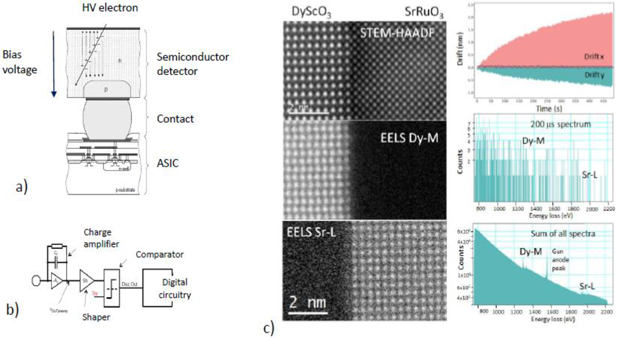
On left, images (a and b) represent a schematic of Medipix3 pixel architecture. In a) the primary electron enters a few hundred microns silicon layer. Electron hole pairs are created. Either electron or hole drift towards the contact at the bottom, upon bias polarity. In b) an analog front end transform the current into a voltage. When it reaches the threshold, a digital counter is incremented. At the end of exposure time, this counter transferred to a computer. On right 6c) a typical experiment on DyScO3/SrRuO3 interface using a Nion UltraSTEM 100 kV 30 mrad probe with 10 pA is displayed. Left images show a sum of 101 scans on the area while drift is measured and canceled online. No post processing is done. Top right image is the actual drift during whole exposure. Middle right image is a single spectrum on a single scan on a pixel. Dwell time per pixel is 200 μs, pixel size is 40 × 40 pm and total experiment time is 8 minutes. The sum averages all scan noises. The Dy-Dy zig-zag chain of 70 pm is clearly visible in HAADF and Dy map (courtesy Marcel Tencé and Alexandre Gloter).
Current usage metrics show cumulative count of Article Views (full-text article views including HTML views, PDF and ePub downloads, according to the available data) and Abstracts Views on Vision4Press platform.
Data correspond to usage on the plateform after 2015. The current usage metrics is available 48-96 hours after online publication and is updated daily on week days.
Initial download of the metrics may take a while.