| Issue |
Eur. Phys. J. Appl. Phys.
Volume 100, 2025
Special Issue on ‘Imaging, Diffraction, and Spectroscopy on the micro/nanoscale (EMC 2024)’, edited by Jakob Birkedal Wagner and Randi Holmestad
|
|
|---|---|---|
| Article Number | 9 | |
| Number of page(s) | 10 | |
| DOI | https://doi.org/10.1051/epjap/2025007 | |
| Published online | 20 March 2025 | |
https://doi.org/10.1051/epjap/2025007
Original Article
Advances in atomic resolution secondary electron imaging
1
Bruker AXS LLC, 11511 NE 118th St, Kirkland, WA 98034, USA
2
Institute of Scientific Instruments of the Czech Academy of Sciences, Královopolská 147, Brno, Czech Republic
3
Department of Mechanical Engineering and Materials Science, Yale University, New Haven, CT 06520, USA
4
Department of Physics & Center for the Science of Materials, Humboldt-Universität zu Berlin, 12489 Berlin, Germany
5
Department of Physics, Arizona State University, Tempe, AZ 85287, USA
* e-mail: This email address is being protected from spambots. You need JavaScript enabled to view it.
** e-mail: This email address is being protected from spambots. You need JavaScript enabled to view it.
Received:
2
November
2024
Accepted:
17
February
2025
Published online: 20 March 2025
Abstract
We have developed an efficient detector of secondary electrons (SEs) for a high-performance scanning transmission electron microscope (STEM) and tested it on several materials. Using the detector at 60 keV, we resolved the nearest neighbor atoms separated by 0.142 nm in SE images of graphene, and detected single-atom substitutions in graphene and monolayer MoS2. We imaged single heavy atoms on an amorphous carbon thin film, and the surface structure of gold nanoparticles supported on a thin film as well as on a bulk substrate. Other application examples shown in this paper include SE imaging combined with 4D STEM, simultaneous SE and electron energy loss spectroscopy (EELS) imaging, and simultaneous imaging of entrance and exit sides of a sample using two separate SE detectors. The results point to an exciting future for atomic-resolution SE imaging.
Key words: Atomic-resolution / secondary-electron-imaging / multi-modal-imaging / 2D-materials
Joel Martis and Benjamin Plotkin-Swing contributed equally to this work.
© J. Martis et al., Published by EDP Sciences, 2025
 This is an Open Access article distributed under the terms of the Creative Commons Attribution License https://creativecommons.org/licenses/by/4.0 which permits unrestricted use, distribution, and reproduction in any medium, provided the original work is properly cited.
1 Introduction
Scanning electron microscopes (SEMs), introduced commercially in the 1960s, [1] are widely used in materials science. In a typical SEM, a focused primary electron beam with an energy between 0.1 and 30 keV is raster scanned across a sample, and low energy (0–50 eV) secondary electrons (SEs) ejected from the sample are used to form SE images. The images are surface-sensitive and contain a wealth of information related to surface properties such as topography and surface potential [2–5]. The resolution of the images is largely determined by the diameter of the focused probe, which is typically 1 nm or greater in modern SEMs, but can be improved to around 0.3 nm by immersing the sample in the magnetic field of an objective lens designed for minimum aberrations.
Atoms on surfaces are typically separated by less than 0.3 nm, and standard SEMs cannot resolve them. The inability to achieve atomic resolution seems to be accepted in the SEM field.
Progressing to <0.2 nm resolution, as necessary for resolving atomic structures, becomes possible by the use of three optical elements: an aberration corrector [6–8], an immersion objective lens, and a low energy spread electron source. This suggests that resolving the atomic structure of surfaces should be possible in instruments using these three elements plus an SE detector.
Modern scanning transmission electron microscopes (STEMs) typically employ all the three elements, and atomic resolution has been demonstrated using an SE detector in an aberration-corrected STEM [9]. Subsequent studies have demonstrated important SE imaging results such as surface structure determination [10] and SE imaging of the atomic structure of the surfaces of bulk samples [11]. Theoretical investigations of the mechanism of SE imaging have proposed high energy ionization events as the origin of the atomic resolution SE signal [12,13].
The above studies performed SE imaging at primary energy Eo of 200 keV. There should be several benefits to imaging at lower energies of the order of 20–100 keV, i.e. closer to the primary energies used by regular SEMs. These energies are compatible with forming <0.2 nm diameter electron probes [14,15], and they lead to:
Increased inelastic cross-sections [16], which are approximately proportional to 1/Eo,
Improved ultimate resolution − inelastic scattering is better localized at lower primary energies [17],
Greatly reduced knock-on damage [18].
Here we demonstrate atomic resolution SE imaging at 60 and 100 keV in a 30-200 keV Nion HERMES STEM by Bruker, equipped with a newly developed SE detector [19]. This STEM also benefits from an ultra-high vacuum (UHV) sample chamber operating at 1 × 10⁻⁹ Torr or better, and in-situ surface cleaning that employs laser heating [20].
2 Materials and methods
Experiments were performed in a Nion HERMES 30-200 keV STEM by Bruker, equipped with a C3-C5 aberration corrector capable of correcting all aberrations up to and including 5th order [21,22], and a monochromator that can decrease the energy width of the electron beam to <5 meV [23,24]. A secondary electron detector based on the Everhart-Thornley design [25] was integrated into the lower (entrance) polepiece of the objective lens (Fig. 1). The detector [19] uses an electrostatic deflector to direct low energy electrons towards a scintillator attached to a light pipe mounted in the lower polepiece. The scintillator is biased to about +10 kV, and the light pipe is coupled to a photomultiplier tube (PMT) mounted on the side of the column. The overall design allows a second SE detector to be integrated into the upper pole-piece in a symmetric configuration.
Secondary electrons spiral towards the detector in the intense magnetic field of the objective lens, but can diverge sideways in regions with no magnetic field and hit the polepiece bore. To prevent this, we typically bias the sample to about −60 V, which keeps the SEs moving towards the detector even in zero field. Backscattered electrons are rejected by an aperture that blocks most of the backscattered signal that enters the lens bore.
For the 4-dimensional (4D) STEM experiments described in this paper, we used a Dectris ARINA − a hybrid pixel direct detector capable of up to 100k frames per second [26] that operates efficiently in the energy range we typically use: 20 to 200 keV. Electron energy loss spectroscopy (EELS) data was recorded using a Nion Iris spectrometer equipped with a Dectris ELA hybrid pixel direct detector [27].
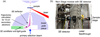 |
Fig. 1 Secondary electron (SE) detector in the Nion HERMES. (a) Schematic showing the SE detector in the lower polepiece of the objective lens, with deflectors guiding low energy secondary electrons towards a scintillator. (b) Photograph of the SE detector and laser illumination system incorporated into the sample stage module of a Nion HERMES. |
3 Results
3.1 SE imaging of gold nanoparticles and atoms on carbon film
As a first test of our SE detector, we imaged gold nanoparticles on carbon film. The sample had many gold nanoparticles deposited on a ∼20 nm thick holey carbon film, purchased from Electron Microscopy Sciences.
Figure 2a shows an SE image of a gold nanoparticle acquired at 60 keV with a 30 mrad convergence semi-angle, and Figure 2b shows a simultaneously acquired high-angle annular dark field (HAADF) image with a 90–200 mrad collection angle. Atoms arranged in rows separated by 0.235 nm are clearly resolved in both the SE and HAADF images.
Figures 2c and 2d show simultaneously acquired SE and HAADF images of gold atoms located on the carbon film between the nanoparticles. Individual atoms are resolved in both types of images, but the contrast in the SE image is lower.
Figure 2e demonstrates that atomic resolution SE imaging can be performed on samples that are thicker than the electron mean penetration depth. It shows an SE image of gold particles resting on a copper grid bar about 50 μm thick, recorded at 100 keV with a 30 mrad convergence semi-angle. Even though the contrast is lower than for gold particles on a thin C film, the image shows clearly resolved atomic rows.
To verify that our SE detector does not collect a significant signal from backscattered electrons, we also imaged gold particles on the 20 nm thick C film that were facing away from the detector, at 100 keV. The HAADF image of the sample in this configuration (Fig. 2g) shows gold particles everywhere, imaged through the supporting film. The corresponding SE image (Fig. 2f) shows no gold particles except next to the hole in the carbon film. The absence of the gold particles in the SE image demonstrates that the SE signal arises from the first few nanometers of the sample facing the SE detector, and that backscattered electrons do not visibly contribute to the image.
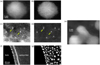 |
Fig. 2 SE and HAADF images of gold nanoparticles: (a) and (b) Simultaneously acquired SE and HAADF images of gold nanoparticles. (c) and (d) Simultaneously acquired SE and HAADF images of individual gold atoms on the carbon film. (e) SE image of gold nanoparticles on a thick copper grid bar. (f) and (g) Simultaneously acquired SE and HAADF images of gold nanoparticles on an amorphous carbon film with the particles facing away from the SE detector. |
3.2 Simultaneous SE and 4D STEM imaging of vanadium-doped monolayer MoS2
Ever since their discovery, 2D materials have been widely explored for their unique and tunable electronic properties with applications in electronic devices, catalysis and photonics [28–31]. Atomic resolution SE imaging of 2D materials should be able to provide unique insights not easily accessible through other imaging methods. We have therefore explored the feasibility of atomic resolution SE imaging of 2D materials, starting with vanadium-doped monolayer MoS2 in which vanadium atoms replace molybdenum ones [32]. The experiments were performed at 60 keV with 35 mrad convergence semi-angle and 15 pA beam current, collecting 4D STEM data simultaneously with the SE and HAADF signals.
Figure 3 shows simultaneously acquired SE, MAADF+ HAADF, and 4D STEM images of monolayer MoS2. A series of 50 scans was acquired, each scan consisting of 170 × 170 pixels, with the pixel dwell time set to 30 μs. Post acquisition, frames were aligned and summed. The MAADF+HAADF image (Fig. 3b) was constructed by summing the traditional HAADF signal with a virtual MAADF signal derived from the 4D STEM image, with the summed image corresponding to a collection angle of 40–200 mrad. All images were processed with single smoothing Gaussian filters.
The bright peaks in the MAADF+HAADF image correspond to Mo atoms (Z = 42), and the much fainter peaks to two S atoms (Z = 16) superimposed in projection. The intensity of the two types of atoms is also different in the SE image (Fig. 3a). The atomic resolution SE signal comes from localized energy loss events [12,13], and as explained in Section 3.3, the signal is expected to be proportional to the relevant core-loss EELS cross sections times the energy loss. This is the reason why Mo atoms are brighter than two superimposed S atoms in the SE image.
The images reveal several deviations from perfect MoS2, with varying visibility in the different images:
A vanadium (V, Z = 23) dopant atom replacing molybdenum (indicated by a yellow arrow).
Sulfur vacancies (indicated by blue arrows), which remove one sulfur atom from an overlapping pair of S atoms.
A line defect consisting of multiple sulfur vacancies (indicated by green arrows). This kind of defect arises by electron beam irradiation creating sulfur vacancies, which then coalesce into linear defects [33].
The SE image clearly shows all these features, demonstrating single atom elemental discrimination. The Mo atoms are much brighter than the substitutional V atom. Two superimposed S atoms are also brighter than the V atom, and much brighter than single S atoms (remaining at the location of a sulfur vacancy).
Figures 3c–3f show images derived from the 4D STEM dataset: a virtual bright field image (Fig. 3c), the integrated differential phase contrast (iDPC) image (Fig. 3d), the center of mass (CoM) image (Fig. 3e) corresponding to the projected electric field [34], and the charge density image (Fig. 3f). In the BF image, the V atom has about the same intensity as the double S atoms, making it difficult to identify the V substitution unambiguously. In the phase and charge density images, the V can be identified, but the Mo and double S images have similar intensity. However, the complete set of six images identifies the different sample features unambiguously. In thicker samples, images b-f would come from the sample volume and only the SE image would come from the surface.
A fully quantitative analysis of the atomic scale SE image contrast would require many different factors to be taken into account: the contributions of all the primary events involved in SE generation, the delocalization of the SE signal, the probability that a secondary electron originating in a sub-surface layer will reach the sample surface, the probability that a secondary electron that has reached the surface with a given energy and direction escapes from the sample, and the collection efficiency of the detector for SEs of different energies and directions. In this contribution we have focused on new multi-modal imaging capabilities, and we leave a fully quantitative analysis for future work.
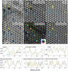 |
Fig. 3 Simultaneously acquired images of vanadium-doped monolayer MoS2: (a) SE, (b) MAADF+HAADF, (c) virtual bright field (BF), (d) phase, (e) transverse electric field worked out by center-of-mass (CoM) analysis, (f) charge density, (g-l) line profiles through a V substitution and an S vacancy along the dashed lines marked in the six images. The transverse electric field profile (k) shows the signal magnitude, and all the signals except the SE one are integrated (projected) in Z. Green arrows point to a line defect, yellow arrow to a substitutional vanadium atom, and blue arrows to sulphur vacancies. Note that atoms are dark in the BF image (c and i), doughnut-like in (the magnitude of) the transverse electric field image (e and k), and bright in all the other images. The arrows and line profile markers are in identical positions in all the images, and the tips of the blue arrows are ∼0.17 nm away from the atomic sites they point to, so that they do not obscure the images of the atoms. |
3.3 SE and EELS imaging of monolayer graphene
The energy that powers the emission of secondary electrons comes from the inelastic scattering of the primary electron beam in the sample, which can be probed by EELS. Comparing an SE image to a simultaneously acquired EELS image is therefore helpful for understanding the contrast of atomic resolution SE images. A classic SE-EELS coincidence study demonstrated that the SE yield per energy loss event is proportional to the energy loss [35], but a comparison of atomically resolved SE and EELS images has not been reported so far. Here we show such a comparison by imaging substitutional atoms in monolayer graphene.
The experiments were performed at 60 keV with a 35 mrad convergence semi-angle, 12 pA probe current, 40–200 mrad MAADF collection angle (using a single MAADF detector), and 40 mrad EELS collection half-angle. The pixel dwell time was set to 220 μs and the scan field to 90 × 90 pixels, which gave a frame time of 1.78 seconds. SE, MAADF and EELS data were acquired simultaneously, and 421 scans were accumulated, for a total acquisition time of 12.5 min. Raw images were up-sampled to 270 × 270 pixels using bilinear interpolation, followed by drift correction and summation. The SE image and the EELS maps were Gaussian-filtered. The MAADF image, whose noise content was unimportant because the up-sampling procedure avoided statistical noise that comes from diving the available signal into many small pixels, was not filtered.
Figures 4a and 4b show SE and MAADF images of monolayer graphene with boron and nitrogen dopants replacing carbon atoms. The B and N atoms are clearly visible in both the images, confirming that even light single impurity atoms can be identified by SE imaging. Figure 4c shows a map of the deposited energy, generated by multiplying the EEL spectrum intensity by the energy loss ΔE, and integrating the product from 1 to 670 eV at each pixel. Figure 4d shows superimposed EELS maps corresponding to the K-edges of C (green), B (red) and N (blue) atoms, verifying their elemental identity.
The deposited energy map shows a strong similarity to the SE image, although subtle differences exist. We also note that in samples thicker than a monolayer, the SE image would show the surface structure whereas the deposited energy map would come from the volume of the sample, and that in samples with different surface and volume structures, there would be no close correspondence between the two types of images.
Figures 4e, 4f and 4g show line profiles across the N and B dopants for the MAADF and SE images, and the deposited energy map. The profiles show that nearest neighbor carbon atoms, separated by just 0.142 nm, are resolved in the SE image. They confirm that the heavier N atom absorbs more energy from the primary beam than C atoms and produces a brighter SE image, whereas the lighter B atom does the opposite. They also reveal that the atomic contrast of the SE image (around 3%) is about ten times lower than the contrast of the MAADF image, but is comparable to the contrast of the deposited energy map. The relative lack of contrast in the SE image and the deposited energy map indicates that individual atoms imaged by these two techniques give rise to a narrow peak that makes atomic resolution imaging possible, plus a broader “skirt” that is due to delocalized scattering. The slight decrease in the contrast of the deposited energy map relative to the SE image is probably due to the map covering energy losses only up to 670 eV, for practical reasons, and the collection half-angle being 40 mrad. Contributions to the map from energy losses >670 eV and large scattering angles would have provided high contrast, and therefore increased the contrast in the map. We plan to evaluate the relative importance of these contributions in the future.
The similarity of the SE image to the deposited energy map prompted us to explore the map’s contrast as a function of the deposited energy. This showed that atomic resolution contrast is already present in maps corresponding to losses of 1–40 eV (encompassing the plasmon loss region), at about 1.3% contrast level. Energies corresponding to inner shell ionizations for B, C and N showed stronger contrast levels: up to 12%. However, the cross sections for inner shell ionizations are small, and this decreases their contribution to the contrast of the deposited energy map. We found that in monolayer graphene, roughly 60% of the atomic resolution contrast in the energy map came from energy loss events higher than 285 eV (the C K-edge threshold energy), and 40% from events below 285 eV.
Atomic resolution contrast of a few percent in low loss EELS images has been observed in graphene previously [36] and its variation with the energy loss explored. The overall picture is that it contributes strongly to the SE image contrast, but not as much as inner shell ionizations.
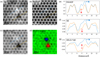 |
Fig. 4 Simultaneous atomic resolution SE, MAADF and EELS imaging of monolayer graphene with boron and nitrogen dopants. (a) SE image, (b) MAADF image, (c) deposited energy map and (d) EELS map corresponding to the K-edges of carbon (green), boron (red) and nitrogen (blue). (e), (f) and (g) Line profiles across the N and B dopants corresponding to MAADF, SE and deposited energy images, taken along the dashed lines shown in the images. |
3.4 Simultaneous imaging of entrance and exit surfaces
Our design allows a second SE detector to be installed on the exit side of the sample. This configuration makes it possible to record SE images of the entrance and exit faces of the sample simultaneously. It is especially powerful when imaging ultrathin (few-layer) samples.
Figure 5 shows images of a linear defect in MoS2 that is like the defect shown in Figure 3, but much longer. Figures 5a and 5b show images formed with the entrance-face and exit-face SE signals, and Figure 5c is an MAADF image, acquired simultaneously with the SE images. The acquisition parameters were: 60 keV primary energy, 40 pA beam current, 35 mrad convergence half-angle, 40–200 mrad MAADF collection angle (using a single MAADF detector), 1 μs dwell time per pixel, 512 × 512 pixels, 1000 scans aligned and summed, cropped to 323 × 478 pixels (to highlight the central area of the image which is of greatest interest), and images (a) to (c) were Gaussian-filtered. Note that because the entrance and exit SE images were acquired simultaneously, their orientation relative to the sample is the same (i.e., the exit image is not mirror-flipped).
Linear defects in MoS2 are believed to have an out-of-plane ‘buckled’ structure, predicted by density functional theory (DFT) relaxation of an atomic model of monolayer MoS2 with a row of S vacancies [33]. Two types of structure were predicted for the defect, and our MAADF image (Fig. 5c) shows that the one examined here was “type II” (Fig 5d). The SE signal is sensitive to the local topography, and the buckling is very likely why the image contrast is different on the left and the right sides of the defect in images acquired with the entrance face SEs (Fig. 5a) and exit face SEs (Fig. 5b). The line profiles show that the ‘topography contrast’ has a characteristic half-width of about 0.5 nm, plus a skirt that extends several nm to one side of the defect, and that increased image intensity next to the defect in the entrance side image corresponds to a slightly decreased intensity in the exit side image. The correspondence is very likely due to sample topography: ridges on sample surfaces emit SEs more efficiently than the planar regions of the sample, and the corresponding valleys on the opposite side emit SEs less efficiently.
In another example of simultaneous use of the entrance and exit face SE detectors, we imaged twisted bilayer MoS2 with a 5 degree twist angle. The acquisition parameters were: 60 keV primary energy, 40 pA beam current, 35 mrad convergence half-angle, 40–200 mrad MAADF collection angle (using a single MAADF detector), 1 μs dwell time per pixel, 1000 scans aligned and summed. All the images of Figure 6 were Gaussian-filtered.
Figure 6a shows the entrance SE image and Figure 6b the exit SE image. Figure 6c shows the MAADF image, in which the moiré pattern created by the twist is very apparent.
The twist allows the image contributions due to the entrance and exit MoS2 layers to be separated. The entrance layer contributes more strongly to the entrance detector image, and the exit layer contributes more strongly to the exit image. Figure 6d shows superimposed images of the boxed sub-areas of Figures 6a (in blue) and 6b (in green). It demonstrates that in a part of the image in which the two layers are staggered with respect to each other such that the Mo atoms of layer 1 overlap the S atoms of layer 2, the Mo atoms belonging to each layer can be identified: their projections alternate around each 6-fold ring.
Fourier transforms of the SE images allowed the strength of the image modulations due to the two layers to be evaluated by measuring the intensities of the well-separated FFT spots due to the two layers. This showed that the far layer’s contribution to the image was only 0.55±0.02 times as strong as the near layer’s contribution, for both the entrance-side and the exit-side images. This implies that there is a sizeable attenuation of the SE signal even through just one monolayer, i.e. that SE imaging is indeed very surface-sensitive.
Subtracting the exit detector image scaled by 0.55 times from the entrance one essentially removes the layer 2 contribution to the image, as shown in Figure 6e. Subtracting 0.55x the entrance image from the exit one removes the layer 1 contribution (Fig. 6f). The purified images make the twist of layer 2 relative to layer 1 very visible.
The layer facing the detector contributes 100/(1+ 0.55) = 65% to the total 2-layer image intensity in both the entrance-side and the exit-side SE images. Using the same layer-to-layer attenuation factor (0.55) to model thicker samples shows that in MoS2 thicker than 10 layers, 45% of the signal would come from the top layer and 70% from the first two layers, i.e. from the first 1.2 nm of the sample.
A short time after our first publication on SE imaging of bilayer MoS2 with 5° twist angle [37], SE images of MoS2 bilayer with 30° twist angle acquired at 200 keV were reported by Saitoh et al. [38,39]. This work found that FFT spots from the second layer were attenuated by a factor of 0.38 ± 0.09 compared to the first layer, in contrast to the attenuation factor of 0.55 ± 0.02 reported here. The difference may be due to the 30° twist producing a more complete shadowing of the second layer by the first one than a 6° twist. We also note that the use of 60 keV produced lower-noise SE images compared to Saitoh et al.’s 200 keV results, in line with our expectations of higher cross-sections when working with lower energy beams.
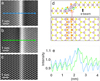 |
Fig. 5 A line defect in MoS2 imaged with (a) entrance face SE, (b) exit face SE, and (c) MAADF. The line defect is believed to have an out-of-plane “buckled” structure as shown in (d), which was adapted from reference [32]. (e) Line profiles through the entrance (blue) and exit face (green) SE images. |
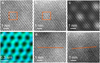 |
Fig. 6 Twisted bilayer MoS2 simultaneously imaged with (a) entrance, and (b) exit side SE, and (c) MAADF. (d) is a composite of the boxed regions in (a) and (b), with the entrance and exit contributions shown in blue and green. (e) and (f) are linear combinations of the entrance and exit signals that suppress the signal from the far layer of the sample, which makes the lattice orientations (indicated by orange lines) and the 5° twist angle readily visible. |
4 Discussion
Our results confirm that when using the SE signal, aberration-corrected STEMs (and SEMs, when they become capable of better than 0.2 nm resolution) can resolve individual atoms on the surfaces of thin as well as thick and even bulk samples. They indicate that high quality SE images can be obtained at primary energies of 100 keV and lower, and that the best operating energy for atomic-resolution SE imaging is likely to be the lowest one at which an atom-sized probe can be formed by the microscope. Here we worked at 60-100 keV, and we plan to explore SE imaging at 30 and 20 keV in the future. These are primary energies at which the Nion HERMES STEM can still resolve the near-neighbor pairs of atoms in graphene [24], separated by 0.142 nm. Good spatial resolution at low primary energies is primarily due to two capabilities available in this microscope: the correction of high order aberrations and the ability to monochromate the illuminating beam without broadening it [24].
Even though the spatial resolution of the SE images was sufficient to resolve the near-neighbor atoms in graphene, it was not as good as the resolution of simultaneously acquired images using the elastic scattering signal, such as HAADF, MAADF, BF, and 4D STEM. This is not unexpected, as the resolution of SE images is limited by the delocalization of the primary inelastic scattering, which causes resolution loss [17] that is similar to the resolution loss seen here for SE imaging.
SE imaging of MoS2 showed that it can identify different types of single-atom surface defects, and it illustrated the value of multi-modal STEM imaging. Simultaneous imaging and EELS analysis of B and N substituting for individual C atoms in graphene showed that single light atoms can be detected by SE imaging, and demonstrated a close correspondence between SE images and maps of the energy deposited into ultra-thin samples. Analyzing this correspondence in more detail showed that about 60% of the atomic resolution contrast in total deposited energy maps and SE images came from inner shell loss ionization, and the rest comes from lower energy inelastic scattering. The analysis also showed that in graphene, the atomic-scale modulation of the SE signal is much weaker than the modulation of the MAADF image. Being able to detect the SE signal from individual light atoms in a graphene sheet is a testament to the efficiency of modern electron microscopes.
SE imaging of a MoS2 monolayer with a linear defect that produced mild buckling of the surface revealed a major difference between the images from one side of the defect and the other side, which we plan to explore further, by recording a series of images of the sample tilted by different amounts. The difference was almost undetectable in the SE image of a shorter version of the same defect (shown in Fig. 3), and this is probably because short versions of the defect do not develop the full buckling illustrated in Figure 5d.
SE imaging of twisted bilayer MoS2 demonstrated that the contribution of sub-surface layers to the total SE image becomes quantifiable in samples in which different layers can be distinguished. Extrapolating to thicker MoS2 samples, we calculated that 45% of the atomic resolution SE signal would come from the first layer, while contributions from layers deeper than 1.2 nm would be less than 1/3 of the total signal. However, it needs to be noted that this result only applies to multi-layer MoS2. In other materials such as metals in which electrons of SE energies can travel long distances, the average escape depth of SE electrons could be substantially different.
While working on the experiments presented here, we repeatedly witnessed the importance of clean surfaces for SE imaging: a single monolayer of contamination typically made surfaces unrecognizable. Keeping contamination at bay is a common problem of all surface analysis techniques. Our approach of a) designing the sample chamber of the microscope for ultra-high vacuum (UHV) operation, and b) providing in-situ cleaning using a laser beam focused on a small area of the sample, has been validated by the quality of the results we have obtained.
5 Summary
We have developed a new SE detector and integrated it into a Nion HERMES STEM. Results obtained with the detector have confirmed that SE imaging provides a valuable addition to the STEM’s analytical powers.
The results have demonstrated that SE imaging can detect single surface atoms including light ones, and confirmed that atomic resolution can be retained when imaging the surfaces of bulk samples. Combining SE imaging with other techniques such as 4D STEM yielded more insights than if each technique were applied separately. When SE imaging was combined with the analysis of the deposited energy, the results showed that the atomic resolution SE contrast is partly due to inner shell loss ionization, and partly due to lower energy loss events. Simultaneous imaging with detectors on the entrance and exit sides of the sample revealed topographic contrast due to the buckling of monolayer MoS2 near a linear defect, and allowed a detailed exploration of the contribution of sub-surface layers to SE images.
Our results demonstrate that SE imaging has much promise for atomic scale surface analysis.
Acknowledgments
We thank George J. Corbin for help in designing the laser illumination module and in the construction of the SE detectors, Benedikt Haas and Christoph Koch for providing us with their 4D STEM analysis code, and Andreas Mittelberger for porting it into the Swift environment.
Funding
This work was mainly supported by R&D funding provided by Nion Co. and Bruker Corp. T.R. acknowledges funding from the Czech Science Foundation (project 21-13541S), and G.A.-S. acknowledges funding from the Deutsche Forschungsgemeinschaft (DFG Projektnummer: 451037016 (PReGrAM)).
Conflicts of interest
J.M., B.P.S., M.T.H., N.D., T.C.L., S.C.Q. and O.L.K. are employees of Bruker A.X.S. L.L.C.
Author contribution statement
O.L.K. and T.R. initiated the S.E. detector development, O.L.K. and M.T.H. did the conceptual and mechanical design of the detector, and T.R. calculated its optical properties. M.T.H. and J.M. built the first prototype, and B.P.S. and M.T.H. built the second detector. O.L.K., G.J.C., J.M. and B.P.S. designed and integrated the laser module. J.M. and T.L. guided the selection of interesting samples, which were prepared by C.S. and G.A.S. N.D. and S.C.Q. set the microscope up for high resolution imaging, and J.M., B.P.S. and M.T.H. acquired and processed the data. All authors contributed to writing the manuscript.
References
- C.W. Oatley, The early history of the scanning electron microscope, J. Appl. Phys. 53, R1 (1982) [Google Scholar]
- L. Reimer, Scanning Electron Microscopy: Physics of Image Formation and Microanalysis (Springer, Berlin, Heidelberg, 1998), Vol. 45 [Google Scholar]
- I. Volotsenko et al., Secondary electron doping contrast: theory based on scanning electron microscope and Kelvin probe force microscopy measurements, J. Appl. Phys. 107, 014510 (2010) [Google Scholar]
- R. Le Bihan, Study of ferroelectric and ferroelastic domain structures by scanning electron microscopy, Ferroelectrics 97, 19 (1989) [Google Scholar]
- J. Li et al., Scanning secondary-electron microscopy on ferroelectric domains and domain walls in YMnO3, Appl. Phys. Lett. 100, 152903 (2012) [Google Scholar]
- N. Dellby, O.L. Krivanek, P.D. Nellist, P.E. Batson, A.R. Lupini, Progress in aberration-corrected scanning transmission electron microscopy, J. Electron Microsc. 50, 177 (2001) [Google Scholar]
- P.E. Batson, N. Dellby, O.L. Krivanek, Sub-ångstrom resolution using aberration corrected electron optics, Nature 418, 617 (2002) [Google Scholar]
- L.M. Brown, P.E. Batson, N. Dellby, O.L. Krivanek, Brief history of the Cambridge STEM aberration correction project and its progeny, Ultramicroscopy 157, 88 (2015) [CrossRef] [PubMed] [Google Scholar]
- Y. Zhu, H. Inada, K. Nakamura, J. Wall, Imaging single atoms using secondary electrons with an aberration-corrected electron microscope, Nat. Mater. 8, 808 (2009) [Google Scholar]
- J. Ciston et al., Surface determination through atomically resolved secondary-electron imaging, Nat. Commun. 6, 7358 (2015) [CrossRef] [Google Scholar]
- S. Hwang et al., Secondary-electron imaging of bulk crystalline specimens in an aberration corrected STEM, Ultramicroscopy 261, 113967 (2024) [CrossRef] [PubMed] [Google Scholar]
- H.G. Brown, A.J. D'Alfonso, L.J. Allen, Secondary electron imaging at atomic resolution using a focused coherent electron probe, Phys. Rev. B 87, 054102 (2013) [Google Scholar]
- R.F. Egerton, Y. Zhu, Spatial resolution in secondary-electron microscopy, J. Microsc. 72, 66 (2023) [Google Scholar]
- O.L. Krivanek et al., Gentle STEM: ADF imaging and EELS at low primary energies, Ultramicroscopy 110, 935 (2010) [CrossRef] [Google Scholar]
- O.L. Krivanek et al., Atom-by-atom structural and chemical analysis by annular dark-field electron microscopy (supporting materials), Nature 464, 571 (2010) [Google Scholar]
- R.F. Egerton, Electron Energy-Loss Spectroscopy in the Electron Microscope (Springer US, Boston, MA, 2011) [Google Scholar]
- R.F. Egerton, Limits to the spatial, energy and momentum resolution of electron energy-loss spectroscopy, Ultramicroscopy 107, 575 (2007) [CrossRef] [PubMed] [Google Scholar]
- R.F. Egerton, P. Li, M. Malac, Radiation damage in the TEM and SEM, Micron 35, 399 (2004) [CrossRef] [PubMed] [Google Scholar]
- M.T. Hotz et al., Atomic resolution SE imaging in a 30-200 keV Aberration-corrected UHV STEM, Microsc. Microanal. 29, 2064 (2023) [Google Scholar]
- J. Martis et al., STEM developments: a versatile light injector/collector, fast 4D-STEM, and high energy resolution EELS without compromising beam current, Microsc. Microanal. 30, 2182 (2024) [Google Scholar]
- O.L. Krivanek, N. Dellby, M.F. Murfitt, Aberration Correction in Electron Microscopy, in Handbook of Charged Particle Optics, edited by J. Orloff, 2nd edn. (CRC Press, Boca Raton, 2009), p. 601 [Google Scholar]
- N. Dellby et al., Tuning high order geometric aberrations in quadrupole-octupole correctors, Microsc. Microanal. 20, 928 (2014) [Google Scholar]
- O.L. Krivanek et al., Vibrational spectroscopy in the electron microscope, Nature 514, 209 (2014) [CrossRef] [PubMed] [Google Scholar]
- N. Dellby et al., Ultra-high resolution EELS analysis and STEM imaging at 20 keV, Microsc. Microanal. 29, 626 (2023) [Google Scholar]
- T. Everhart, R.F.M. Thornley, Wide-band detector for micro-microampere low-energy electron currents, J. Sci. Instrum. 37, 246 (1960) [Google Scholar]
- B. Plotkin-Swing et al., 100,000 diffraction patterns per second with live processing for 4D-STEM, Microsc. Microanal. 28, 422 (2022) [Google Scholar]
- B. Plotkin-Swing et al., Hybrid pixel direct detector for electron energy loss spectroscopy, Ultramicroscopy 217, 113067 (2020) [CrossRef] [PubMed] [Google Scholar]
- S. Das et al., Transistors based on two-dimensional materials for future integrated circuits, Nat. Electron. 4, 786 (2021) [Google Scholar]
- M.C. Lemme, D. Akinwande, C. Huyghebaert, C. Stampfer, 2D materials for future heterogeneous electronics, Nat. Commun. 13, 1392 (2022) [Google Scholar]
- Y. Wang et al., Catalysis with two-dimensional materials confining single atoms: concept, design, and applications, Chem. Rev. 119, 1806 (2019) [Google Scholar]
- M. Turunen, M. Brotons-Gisbert, Y. Dai et al., Quantum photonics with layered 2D materials, Nat. Rev. Phys. 4, 219 (2022) [Google Scholar]
- J. Zhang et al., Vanadium-doped monolayer MoS2 with tunable optical properties for field-effect transistors, ACS Appl. Nano Mater. 4, 769 (2021) [CrossRef] [Google Scholar]
- Q. Chen et al., Ultralong 1D vacancy channels for rapid atomic migration during 2D void formation in monolayer MoS2, ACS Nano 12, 7721 (2018) [CrossRef] [PubMed] [Google Scholar]
- K. Müller et al., Atomic electric fields revealed by a quantum mechanical approach to electron picodiffraction, Nat. Commun. 5, 5653 (2014) [Google Scholar]
- H. Mullejans, A.L. Bleloch, A. Howie, M. Tomita, Secondary electron coincidence detection and time of flight spectroscopy, Ultramicroscopy 52, 360 (1993) [CrossRef] [Google Scholar]
- M.D. Kapetanakis et al., Low-loss electron energy loss spectroscopy: an atomic-resolution complement to optical spectroscopies and application to grapheme, Phys. Rev. B 92, 125147 (2015) [Google Scholar]
- B. Plotkin-Swing et al., Atomic resolution secondary electron imaging of top and bottom surfaces, Microsc. Microanal. 30, 1480 (2024) [Google Scholar]
- K. Saitoh, K. Tamaki, Depth sensitivity of atomic resolution secondary electron imaging, in 17th European Microscopy Congress (EMC 2024) (BIO Web of Conferences, 2024). https://doi.org/10.1051/bioconf/202412904028 [Google Scholar]
- K. Saitoh et al., Surface sensitivity of atomic-resolution secondary electron imaging, Microscopy 74, 28 (2025). https://doi.org/10.1093/jmicro/dfae041 [Google Scholar]
Cite this article as: Joel Martis, Benjamin Plotkin-Swing, Michael T. Hotz, Niklas Dellby, Tracy C. Lovejoy, Amber M. Nelson-Quillin, Tomáš Radlička, Cong Su, Gerardo Algara-Siller, Ondrej L. Krivanek, Advances in atomic resolution secondary electron imaging, Eur. Phys. J. Appl. Phys. 100, 9 (2025), https://doi.org/10.1051/epjap/2025007
All Figures
|
Fig. 1 Secondary electron (SE) detector in the Nion HERMES. (a) Schematic showing the SE detector in the lower polepiece of the objective lens, with deflectors guiding low energy secondary electrons towards a scintillator. (b) Photograph of the SE detector and laser illumination system incorporated into the sample stage module of a Nion HERMES. |
| In the text | |
|
Fig. 2 SE and HAADF images of gold nanoparticles: (a) and (b) Simultaneously acquired SE and HAADF images of gold nanoparticles. (c) and (d) Simultaneously acquired SE and HAADF images of individual gold atoms on the carbon film. (e) SE image of gold nanoparticles on a thick copper grid bar. (f) and (g) Simultaneously acquired SE and HAADF images of gold nanoparticles on an amorphous carbon film with the particles facing away from the SE detector. |
| In the text | |
|
Fig. 3 Simultaneously acquired images of vanadium-doped monolayer MoS2: (a) SE, (b) MAADF+HAADF, (c) virtual bright field (BF), (d) phase, (e) transverse electric field worked out by center-of-mass (CoM) analysis, (f) charge density, (g-l) line profiles through a V substitution and an S vacancy along the dashed lines marked in the six images. The transverse electric field profile (k) shows the signal magnitude, and all the signals except the SE one are integrated (projected) in Z. Green arrows point to a line defect, yellow arrow to a substitutional vanadium atom, and blue arrows to sulphur vacancies. Note that atoms are dark in the BF image (c and i), doughnut-like in (the magnitude of) the transverse electric field image (e and k), and bright in all the other images. The arrows and line profile markers are in identical positions in all the images, and the tips of the blue arrows are ∼0.17 nm away from the atomic sites they point to, so that they do not obscure the images of the atoms. |
| In the text | |
|
Fig. 4 Simultaneous atomic resolution SE, MAADF and EELS imaging of monolayer graphene with boron and nitrogen dopants. (a) SE image, (b) MAADF image, (c) deposited energy map and (d) EELS map corresponding to the K-edges of carbon (green), boron (red) and nitrogen (blue). (e), (f) and (g) Line profiles across the N and B dopants corresponding to MAADF, SE and deposited energy images, taken along the dashed lines shown in the images. |
| In the text | |
|
Fig. 5 A line defect in MoS2 imaged with (a) entrance face SE, (b) exit face SE, and (c) MAADF. The line defect is believed to have an out-of-plane “buckled” structure as shown in (d), which was adapted from reference [32]. (e) Line profiles through the entrance (blue) and exit face (green) SE images. |
| In the text | |
|
Fig. 6 Twisted bilayer MoS2 simultaneously imaged with (a) entrance, and (b) exit side SE, and (c) MAADF. (d) is a composite of the boxed regions in (a) and (b), with the entrance and exit contributions shown in blue and green. (e) and (f) are linear combinations of the entrance and exit signals that suppress the signal from the far layer of the sample, which makes the lattice orientations (indicated by orange lines) and the 5° twist angle readily visible. |
| In the text | |
Current usage metrics show cumulative count of Article Views (full-text article views including HTML views, PDF and ePub downloads, according to the available data) and Abstracts Views on Vision4Press platform.
Data correspond to usage on the plateform after 2015. The current usage metrics is available 48-96 hours after online publication and is updated daily on week days.
Initial download of the metrics may take a while.