| Issue |
Eur. Phys. J. Appl. Phys.
Volume 85, Number 1, January 2019
|
|
|---|---|---|
| Article Number | 10102 | |
| Number of page(s) | 9 | |
| Section | Semiconductors and Devices | |
| DOI | https://doi.org/10.1051/epjap/2018180282 | |
| Published online | 22 February 2019 | |
https://doi.org/10.1051/epjap/2018180282
Regular Article
Measure and analysis of 4H-SiC Schottky barrier height with Mo contacts
UDL, INSA Lyon, Universite Claude Bernard Lyon 1, Ecole Centrale de Lyon, CNRS,
Ampere,
69621
Villeurbanne,
France
* e-mail: This email address is being protected from spambots. You need JavaScript enabled to view it.
Received:
28
September
2018
Received in final form:
14
December
2018
Accepted:
20
December
2018
Published online: 22 February 2019
Abstract
Current–voltage (I–V) and capacitance–voltage (C–V) characteristics of Schottky Mo/4H-SiC diodes have been measured and analyzed as a function of temperature between 80 and 400 K. The I–V characteristics significantly deviate from ideal characteristics predicted by the thermionic emission model because of the inhomogeneity of Schottky contact. After a brief review of the different existing models, the main parameters (ideality factor, barrier height, and effective Richardson constant) of both diodes have been extracted in the frame of a Gaussian barrier height distribution model, whose mean and standard deviation are linearly dependent on voltage and temperature, as well as in the context of the potential fluctuation model. The results are compared with the values extracted by C–V and the values in the literature. A link is established between these two models. Diodes of different I–V characteristics, either identified as single barrier or double barrier, have been analyzed by Deep Level Transient Spectroscopy (DLTS) to investigate the deep level defects present. No noticeable difference has been found.
© EDP Sciences, 2019
1 Introduction
Since many years, it has been observed that the current–voltage (I–V) characteristics of Schottky diodes on SiC are rarely correctly modeled by a simple model of thermionic injection of electrons over a barrier height [1,2]. This phenomenon is also observed in Schottky on inorganic semiconductor [3]. The thermionic-emission (TE) model gives the forward current I through the diode by the formula: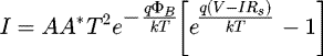 (1)where V is the voltage across the Schottky diode, R
s
is its series resistance (including resistance of epitaxial, substrate, and back face Ohmic contact), A the surface of Schottky contact, A
* the effective Richardson constant, T the temperature, Φ
B
the barrier height of the Schottky contact that is assumed constant, q the elementary charge, and k the Boltzmann constant. The term preceding the brackets is called saturation current I
s
. In the region where R
s
is negligible and V > 3kTq, the relationship can be simplified as:
(1)where V is the voltage across the Schottky diode, R
s
is its series resistance (including resistance of epitaxial, substrate, and back face Ohmic contact), A the surface of Schottky contact, A
* the effective Richardson constant, T the temperature, Φ
B
the barrier height of the Schottky contact that is assumed constant, q the elementary charge, and k the Boltzmann constant. The term preceding the brackets is called saturation current I
s
. In the region where R
s
is negligible and V > 3kTq, the relationship can be simplified as: (2)
(2)
Therefore, the plot of ln(I) versus V should give a straight line whose slope is q/kT and the intercept with y-axis makes it possible to calculate I s .
In reality, the slope is rarely equal to q/kT and therefore more complex models, ranging from double barrier height models to the Gaussian barrier height distribution as well as models in which Φ B depends on V and/or T have been published [4–6]. Particularly the Gaussian model explains rather well the measurements made on the Schottky diodes with deposit of Mo on 4H-SiC.
We present an analysis of these different models and apply them to the study of molybdenum Schottky contacts on n-type 4H-SiC epitaxies. The I–V and C–V characteristics have been measured between 80 and 400 K and the results have been analyzed to extract in particular the barrier heights and ideality factors.
2 Analytical models
2.1 The ideality factor and the barrier height at 0 V
Considering that the Schottky barrier height (SBH) varies linearly with the voltage as Φ
B
= Φ
B0 + γV, where Φ
B0 is the barrier height at 0 V and γ(= ∂ Φ
B
/∂V) is positive, equation (1) becomes: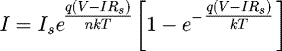 (3)with the saturation current I
s
given by:
(3)with the saturation current I
s
given by: (4)where n = 1/(1 − γ) is recognized as the ideality factor of the diode [7].
According to equations (3) and (4), the relationship between log (I) and V should be linear if the series resistance is small enough to be neglected. Therefore, the ideality factor and the barrier height at 0 V can be determined from the I–V plot.
Hackam and Harrop [8] have proposed that, to take into account, the effect of a thin interfacial layer as well as the effect of image force and the presence of surface charges on the barrier height, which also manifest at 0 V and result in n ≠ 1, it is necessary to integrate the ideality factor into the saturation current as well. Therefore, equation (4) is amended as follows: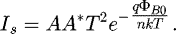 (5)
(5)
2.2 T 0 effect
In order to precisely fit the experimental I–V characteristics of Schottky diodes, where a variation of n with temperature is observed, Padovani and Sumner [9] have suggested to replace T by T + T
0 in the TE model, therefore equation (1) becomes (neglecting R
s
):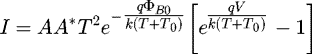 (6)where T
0 neither depends on the temperature nor the voltage over a wide temperature range. Thus, this relation is equal to introduce an ideality factor in the two exponential terms:
(6)where T
0 neither depends on the temperature nor the voltage over a wide temperature range. Thus, this relation is equal to introduce an ideality factor in the two exponential terms: (7)
(7)
2.3 Gaussian distribution of barrier heights
To explain the difference between SBH measured by I–V and C–V over the range of measured temperatures, Song et al. [4] have assumed that the barrier height is normally distributed with a probability density: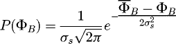 (8)where
  is the mean barrier height and σ
s
is its standard deviation.
is the mean barrier height and σ
s
is its standard deviation.
As a general SBH distribution, equation (8) can also be applied at 0 V (the zero bias condition). In that case, the SBH can be expressed as: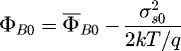 (9)where
  and σ
s0 are the corresponding parameters in Gaussian distribution at 0 V. Practically, the SBH at 0 V Φ
B0 can be calculated at each temperature according to equation (4) if we know the value of A
*. Thus, it is possible to extract
and σ
s0 are the corresponding parameters in Gaussian distribution at 0 V. Practically, the SBH at 0 V Φ
B0 can be calculated at each temperature according to equation (4) if we know the value of A
*. Thus, it is possible to extract  and σ
s0 by tracing Φ
B0 versus q/2kT.
and σ
s0 by tracing Φ
B0 versus q/2kT.
2.4 Potentiel fluctuation model
This model has been developed by Werner and Guttler [5] to explain the temperature dependence of the ideality factor. The barrier height is assumed to be normally distributed, but the mean and standard deviation are assumed to vary linearly with voltage as:
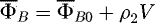 and
and 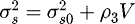 .
.
We can then show that the ideality factor can be expressed in the form: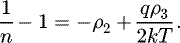 (10)
(10)
By tracing n −1 − 1 versus q/2kT, the values of ρ 2 and ρ 3 are obtained respectively from the slope and the y-intercept.
2.5 Flat-band barrier height
Since the barrier height depends on the bias voltage, i.e. in fact the electric field, Wagner et al. [6] have proposed to define the barrier height under flat-band condition (zero field) Φ
BF
, which would be a more fundamental magnitude due to independence of the applied voltage and is given by: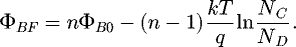 (11)
(11)
2.6 Richardson plot and its modifications
To determine the effective Richardson constant  , the Richardson plot, based on equations (1) and (2),
  versus 1/T should be linear with a slope related to the barrier height and an intercept bound to
  .
.
According to equations (5), (9), and (11), the barrier height is determined from so-called modified Richardson (MR) plots, of which there are several variants. The plot
of  versus 1/nT (Eq. (5), [8]),
 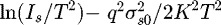 versus q/kT (Gaussian model, [10]) or
  versus 1/nT ([11]) allow to determine the barrier height at 0 V or in flat-band condition.
2.7 C–V characteristics
In the case of an n-type Schottky diode with an uniform doping N
D
− N
A
, the capacitance C is related to the width of the space charge region W: (12)and W relates to the doping concentration by
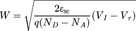 (13)where ϵ
sc is the dielectric permittivity of the semiconductor and V
r
the reverse polarization.
(13)where ϵ
sc is the dielectric permittivity of the semiconductor and V
r
the reverse polarization.
If doping is uniform, the tracing of 1/C
2 = f (V
r
) must be straight, and the intersection V
I
with x-axis gives the barrier height  [12]:
[12]: (14)
(14)
3 Experimental setup
Two n-type Mo/4H-SiC Schottky diodes on the same wafer that were provided by our collaborator have been characterized and noted (a) and (b). The molybdenum anode is in square shape with a surface area of 2.48 mm2. A post-annealing of 500 °C were taken out after the lift-off process during the fabrication. The direct I–V measurements have been made by the 4-cable method (Kelvin method) with Keithley K2410 between 80 and 400 K with a step of 20 K in a cryostat and under darkness. The C–V measurements, between 0 and −5 V, were performed under the same conditions at 100 kHz with a Keysight E4990A impedance analyzer. The analysis of the electrically active defects has then been conducted with a PhysTech FT-1230 High Energy Resolution Analysis Deep Level Transient Spectroscopy (HERA DLTS) bench between 20 and 550 K. The reverse-state voltage is V R = − 10 V and the filling pulse voltage is VP = − 0.1 V for a duration of tP = 100μs for all DLTS tests. Depending on the temperature range, the DLTS technique used is either DLTS in current mode (measure of current transients) at low temperature (20–170 K), or DLTS in capacitance mode at higher temperature (200–550 K) for the propose of optimal precision. In order to avoid an annealing effect under the temperature ramp, a fast preliminary DLTS scan has been carried out on both diodes (from 300 to 550, then back to 300 K for a total of 3 hours).
4 Results and discussion
4.1 Forward I–V characteristics
In Figure 1, the log(I)–V characteristics of the diode (a) are almost linear over the entire temperature range. On the contrary, for the diode (b), the I–V curves clearly show a phenomenon of multi-barrier, especially at low temperature. Indeed, under high current (>10μA) even at 80 K, log(I)–V is linear as for diode (b). While under low voltage, the current is abnormally strong compared to the diode (a), although its variation log(I) versus V also linear up to about 100 nA. Such multi-barrier behavior has been observed by Gelczuck et al. as well [13], who attributed these two parts of the I–V curve to an inhomogeneity of the barrier height, a low SBH L-SBH and a higher SBH H-SBH. In that case, the log(I)–V characteristics can be divided into two linear regions, giving each an ideality factor and a saturation current extracted from equations (3) and (4).
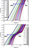 |
Fig. 1 Forward current–voltage characteristics measured on diodes (a) and (b) of Mo/4H-SiC with a surface area of 2.48 mm2 between 80 and 400 K in 20 K increments. |
4.2 C–V characteristics
Figure 2 shows the barrier height and doping concentration extracted from the C–V as a function of temperature.  has a maximum around 200 K. Doping slightly increases with temperature, except for diode (b) at 80 K, which may be due to experimental errors.
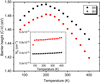 |
Fig. 2 SBH |

4.3 Flat-band barrier height and modified Richardson plot
The MR plot based on the flat-band barrier height is adopted here since it is possible to extract all the parameters involved with the I–V (n, I s ) and C–V curves (N D ).
Although I–V curves appear linear throughout the temperature range for diode (a), the MR plot (Fig. 3a) shows two distinct regions: between 80 and 200 K, Φ BF = 1.20 eV and between 220 and 400 K, Φ BF = 1.50 eV. The diode (b) (Fig. 3b) performs similar barrier heights (1.30 eV between 80 and 160 K, and 1.59 eV between 300 and 400 K). However, it also presents a lower barrier height Φ BF = 0.67 eV on the full extent of temperature (80−400 K). This lower barrier height is responsible for the excess current at low temperature on (b). A * has also been calculated in each linear area of the MR plot using the area A of the diode, and the value obtained is used for subsequent calculations. Another solution would be to use a constant value A * (the higher value extracted, 1.50 eV), and to calculate a ratio between the areas of the high and low SBH regions. The values of A * are substantially different from several orders of magnitude in different regions, therefore the surface ratio is rather small. Even for a ratio of 5.7 × 10⁻¹⁰ (area of the low SBH on the total surface of the diode), its influence on the I–V characteristics cannot be neglected.
For the transition zone between 180 and 280 K on the diode (b), which can result from the coexistence of two different barriers, the value A * adopted is that obtained at high temperature.
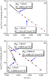 |
Fig. 3 Modified Richardson plot based on flat-band barrier height on diodes (a) and (b). n and I s were calculated in the different linear zones of the I–V curves, and N D is extracted from the C–V characteristics. |
4.4 Gaussian distribution of barrier height
The curves obtained based on the Gaussian model are linear at each region (Fig. 4). The average value of the barrier height with Gaussian distribution therefore appears as the limit at very high temperature. Consider the common SBH of both diode, for high temperature measurements, 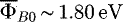 for both while at low temperature
 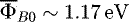 for (a) and
  for (b). The similar H-SBH that dominates at high temperature is close to the barrier that is obtained by C–V. Indeed, the barrier height extracted by C–V is always that corresponds to the region of greater contact area [4]. At low temperatures, the two diodes have distinct behavior and the barrier heights are different, but their temperature variations (i.e. standard deviation σ
s
) in each region are still similar. A more remarkable difference for the tran
sition zone between low and high SBH could be due to the value A
* adopted in the high temperature zone.
for (b). The similar H-SBH that dominates at high temperature is close to the barrier that is obtained by C–V. Indeed, the barrier height extracted by C–V is always that corresponds to the region of greater contact area [4]. At low temperatures, the two diodes have distinct behavior and the barrier heights are different, but their temperature variations (i.e. standard deviation σ
s
) in each region are still similar. A more remarkable difference for the tran
sition zone between low and high SBH could be due to the value A
* adopted in the high temperature zone.
The disadvantage of this model is that it requires to characterize the distribution of barrier height, and to know the value of A *, otherwise either using a value from the literature such as Reddy and Reddy [10] or extracting the value from an MR plot (Sect. 4.3).
 |
Fig. 4 Barrier heights at 0 V as a function of temperature for extraction of parameters in Gaussian distribution on diodes (a) and (b). |
4.5 Potentiel fluctuations model
Figure 5 shows the experimental plot of 1/n − 1 versus q/2kT. The values of ρ2 and ρ3 are determined from the slope and the intercept. Since the ideality factor n can be obtained directly from the I–V curves, thus it can rule out the error from the value of A*, unlike in the Gaussian model.
In the same way as for the Gaussian model, linear zones can be identified and the coefficients ρ 2 and ρ 3 are determined in each zone. Referring to the L-SBH, the coefficients ρ 3 are similar for both diodes (∽−5 mV).
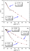 |
Fig. 5 Tracing of 1/n − 1 in terms of q/2kT on the diodes (a) and (b). |
4.6 DLTS measurements
Figure 6 shows the DLTS spectra of the diodes after their I–V and C–V characterizations between 20 and 550 K. The I-DLTS spectra are dominated by two negative peaks between 70 and 170 K, and two other peaks below 60 K. These defects were analyzed by an Arrhenius plot and their characteristics are gathered in Table 1. The characteristics of other defects that appear on capacitance DLTS spectra are given in Table 2.
As we can see in the Figure 6, the DLTS results are rather similar between the two diodes, with the only exception of the peak around 280 K. Considering the uncertainties inherent in the Arrhenius analysis, the energies extracted for this peak are quite close to each other, which means that the defects observed are common on the two Mo diodes.
The physical origin of these defects is specified in Table 3. The two levels at ∽40 K are attributed to nitrogen. Their activation energies and high concentrations correspond well to the values determined in the literature.
The default at 0.15 eV has been attributed to the Ti [24,25] or to the Cr [24–26]. However, apart from unintentional contamination during manufacture, it is difficult to relate this level to Cr or Ti.
The defect Z 1/Z 2 is observed around 280 K, with very low concentrations compared to that measured after radiation (e.g. by protons [18] or Kr ions [19]).
The origins of deeper defects labeled NB and RD1/2 centers are not clear. However, same defect levels detected among Schottky diodes fabricated with various metal contacts on 4H-SiC indicate that their origins are rather related to the SiC than to the metal contact. Similar levels have also been reported by Kawahara et al. after either high temperature oxidation or C+ implantation followed by Ar annealing and labeled as ON1 and ON2, where these levels are assumed to originate from the interstitials generated at the SiO2/SiC interface [27].
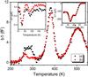 |
Fig. 6 DLTS signal (correlation b1) with a period of 204.8 ms on the diodes (a) and (b) between 200 and 550 K. The inserts are current DLTS (I-DLTS) spectrum between 20 and 60 K (upper right) and 70 to 170 K (top left). The reverse bias V R = − 10 V, the pulse voltage V P = − 0.1 V and the pulse duration t P = 100 s for all measures. |
5 Discussion
5.1 SBH models
The obtained values of Φ
B0, Φ
BF
, and  on both diodes are represented in Figure 7. Φ
B0 varies over the entire temperature range while Φ
BF
almost remains constant, with values close to
on both diodes are represented in Figure 7. Φ
B0 varies over the entire temperature range while Φ
BF
almost remains constant, with values close to  . These Φ
BF
values based on equation (11) at each temperature are in good agreement with the values obtained by the MR plot (Fig. 3).
. These Φ
BF
values based on equation (11) at each temperature are in good agreement with the values obtained by the MR plot (Fig. 3).
The discontinuity of Φ
BF
results from the change in value of A
* in both high and low temperature regions. For the diode (b), the difference between Φ
BF
and  is slightly larger due to errors in the MR plot or doping extracted by C–V.
Consider the T
0 effect where the constant extracted from nT versus T plot with a typical value around 100 K in our case. Therefore, equation (11) is reduced to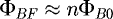 (15)since the second part of the expression
 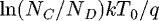 can be neglected. Equation (15) can well explain the MR plot according to equation (5), where the value extracted should be close to Φ
BF
.
can be neglected. Equation (15) can well explain the MR plot according to equation (5), where the value extracted should be close to Φ
BF
.
Therefore, by replacing Φ
B0 by  in equation (9), the relationship between the ideality factor and and the parameters of the Gaussian distribution can be expressed in the form:
 (16)
(16)
Comparing with equation (10), we can show that: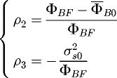 (17)or
 (18)
(18)
This highlights the links between the Gaussian distribution model and the potential fluctuation model. Mean barrier heights and standard deviations calculated according to equation (18) are given in Table 4, as well as the other parameters used in these two models.
The values between the two models are in good agreement, especially for diode (a). On the diode (b) the slight disagreement could come from either the errors related to the linear approximations of the experimental curves or to the approximation of the equation (15).
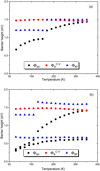 |
Fig. 7 Temperature evolution of the SBH at 0 V Φ B0 extracted from I − V, the SBH extracted from C − V |


5.2 Barrier inhomogeniety
The multi-barrier behavior, performs with an excess of forward current at low voltage bias, has often been reported during SBD characterizations, and it was highlighted that these non-ideal diodes occurred regardless of growth technique, pre-deposition cleaning method, or contact metal [28]. Moreover, this double-barrier was found to be more common at lower temperature, which was explained by barrier height inhomogeneities [13].
In order to well explain the multi-barrier behavior of SBD, the first thing that comes to mind is the parallel diode model, which treats the additional low barrier height region as an individual diode that is responsible for the excess current. This model has been numerically discussed by Brezeanu et al. [29] that can explain the relatively low barrier measured at cryogenic temperature. However, this model does not take into consideration of the interaction between low and common SBH regions and cannot explain the size effect: even with the same area ratio of both high and low SBH regions, the effective barrier height increases when the total size is reduced, especially when the dimensions are comparable or shorter than the Debye length of the substrate [30].
A more widely recognized model for barrier inhomogeneity characterization is the one put forward by Tung, where a set of low barrier patches are introduced that would pinch-off under certain condition [31]. Later, this model has been optimized by Gammon et al. by involving the series resistance, thus the I–V–T data over a wide temperature range can be well reproduced [32].
However, in order to reproduce the I–V characteristics, a number of parameters must be fixed by fitting in the full temperature range with either Tung's model or its modifications. Therefore, it is not realistic for mass testing, and most of time unnecessary. In fact, with the help of MR plot or even simpler, the potential fluctuation model, it is possible to locate those low SBH regions with large effective area where the double-barrier phenomenon usually results from. These patches may attract more attentions and could be identified by optical or other characterizations much easily.
Since no obvious difference has been observed by DLTS under tested bias condition, the multi-barrier behavior is suggested to be caused by extended interface defects (e.g. dislocation or stacking fault). Therefore, interface defects characterization is supposed for further investigations.
6 Conclusion
The two molybdenum-based Schottky diodes have been characterized by I–V, C–V, and DLTS. The MR plot has been adopted to extract barrier height in flat band condition. This circumvents the weak point of the Gaussian distribution model (which requires knowing the value of A*) and improves accuracy over the conventional Richardson plot.
Based on the MR plot, Richardson constants A* have been determined in each operating region. The SBH models, namely Gaussian distribution and potential fluctuation, have been verified and main parameters have been calculated from the determined A * values. Both models are in good agreement.
Conventional DLTS and I-DLTS analysis have been performed between 200 and 550 K and between 20 and 170 K to investigate the presence of deep level defects. Four defects have been detected and identified at low temperatures and five at higher temperatures. The Z1/Z2 defect is present in small concentration. The origin of high temperature defects is not determined, although they are also listed in the literature.
In any case, no particular difference has been revealed between the two DLTS diodes, which means that the multiple barrier phenomenon on the I–V curves does not originate in the deep level defects, at least in this temperature range studied.
In addition, the approximation of Φ BF as a function of Φ B0 and n has been underlined. The result is a link between the Gaussian distribution models and the potential fluctuation model that had not yet been published. The parameters of these two models have been compared using the value of the barrier height in flat band condition, and it appears that the two models are in good agreement.
Authors contribution statement
Teng Zhang performed the IV and DLTS measurements and analyses the results. Christophe Raynaud helped to analyse, interpret and discuss the results. All authors contributed to improving the paper from version to version. Dominique Planson carefully proofread and assisted in editing the manuscript.
Acknowledgments
The authors thank the Chinese government for its financial support through a scholarship from the Chinese Scholarship Council (CSC) no. 201506090154, as well as the National Center of Microelectronics of Barcelona and Caly Technologies for the manufacture/design of the components.
References
- D. Defives, O. Noblanc, C. Dua, C. Brylinski, M. Barthula, V. Aubry-Fortuna, F. Meyer, IEEE Trans. Electron Devices 46, 449 (1999) [Google Scholar]
- C. Raynaud, K. Isoird, M. Lazar, C.M. Johnson, N. Wright, J. Appl. Phys. 91, 9841 (2002) [Google Scholar]
- S. Bandyopadhyay, A. Bhattacharyya, S.K. Sen, J. Appl. Phys. 85, 3671 (1999) [Google Scholar]
- Y.P. Song, R.L.V. Meirhaeghe, W.H. Laflère, F. Cardon, Solid-State Electron. 29, 633 (1986) [CrossRef] [Google Scholar]
- J.H. Werner, H.H. Gttler, J. Appl. Phys. 69, 1522 (1991) [Google Scholar]
- L.F. Wagner, R.W. Young, A. Sugerman, IEEE Electron Device Lett. 4, 320 (1983) [Google Scholar]
- S. Chand, J. Kumar, Semicond. Sci. Technol. 11, 1203 (1996) [Google Scholar]
- R. Hackam, P. Harrop, IEEE Trans. Electron Devices 19, 1231 (1972) [Google Scholar]
- F.A. Padovani, G.G. Sumner, J. Appl. Phys. 36, 3744 (1965) [Google Scholar]
- N.N.K. Reddy, V.R. Reddy, Bull. Mater. Sci. 35, 53 (2012) [CrossRef] [Google Scholar]
- S. Chand, J. Kumar, Semicond. Sci. Technol. 10, 1680 (1995) [Google Scholar]
- E.H. Rhoderick, R.H. Williams, Metal-Semiconductor Contacts , 2nd edn. (Clarendon Press, Oxford, 1988) [Google Scholar]
- L. Gelczuk, P. Kamyczek, E. Paczek-Popko, M. Dbrowska-Szata, Solid-State Electron. 99, 1 (2014) [CrossRef] [Google Scholar]
- F. Nava, A. Castaldini, A. Cavallini, P. Errani, V. Cindro, IEEE Trans. Nucl. Sci. 53, 2977 (2006) [Google Scholar]
- E. Omotoso, W.E. Meyer, S.M.M. Coelho, M. Diale, P.N.M. Ngoepe, F.D. Auret, Mater. Sci. Semicond. Process. 51, 20 (2016) [Google Scholar]
- T. Kimoto, A. Itoh, H. Matsunami, S. Sridhara, L.L. Clemen, R.P. Devaty, W.J. Choyke, T. Dalibor, C. Peppermüller, G. Pensl, Appl. Phys. Lett. 67, 2833 (1995) [Google Scholar]
- A. Uddin, H. Mitsuhashi, T. Uemoto, Jpn. J. Appl. Phys. 33, L908 (1994) [Google Scholar]
- D. Davydov, A. Lebedev, V. Kozlovski, N. Savkina, A. Strel'chuk, Physica B 308-310, 641 (2001) [CrossRef] [Google Scholar]
- E. Kalinina, G. Onushkin, D. Davidov, A. Hallen, A. Kon-stantinov, V.A. Skuratov, J. Stano, Electrical study of 4H-SiC irradiated with swift heavy ions, in 12th International Conference on Semiconducting and Insulating Materials, 2002, SIMC-XII-2002 (IEEE, 2002) [Google Scholar]
- T. Dalibor, G. Pensl, T. Kimoto, H. Matsunami, S. Sridhara, R.P. Devaty, W.J. Choyke, Diam. Relat. Mater. 6, 1333 (1997) [Google Scholar]
- Z.Q. Fang, D.C. Look, A. Saxler, W.C. Mitchel, Physica B 308–310, 706 (2001) [CrossRef] [Google Scholar]
- M. Kato, S. Tanaka, M. Ichimura, E. Arai, J. Appl. Phys. 100, 053708 (2006) [Google Scholar]
- K. Danno, T. Kimoto, H. Matsunami, Appl. Phys. Lett. 86, 122104 (2005) [Google Scholar]
- N. Achtziger, W. Witthuhn, Appl. Phys. Lett. 71, 110 (1997) [Google Scholar]
- N. Achtziger, D. Forkel-Wirth, J. Grillenberger, T. Licht, W. Witthuhn, Nucl. Instrum. Methods Phys. Res. Sect. B 136–138, 756 (1998) [CrossRef] [Google Scholar]
- N. Achtziger, W. Witthuhn, Mater. Sci. Eng. B 46, 333 (1997) [CrossRef] [Google Scholar]
- K. Kawahara, J. Suda, T. Kimoto, J. Appl. Phys. 111, 053710 (2012) [Google Scholar]
- D.J. Ewing, Q. Wahab, R.R. Ciechonski, M. Syvjrvi, R. Yakimova, L.M. Porter, Semicond. Sci. Technol. 22, 1287 (2007) [Google Scholar]
- G. Brezeanu, G. Pristavu, F. Draghici, M. Badila, R. Pascu, J. Appl. Phys. 122, 084501 (2017) [Google Scholar]
- J.L. Freeouf, T.N. Jackson, S.E. Laux, J.M. Woodall, Appl. Phys. Lett. 40, 634 (1982) [Google Scholar]
- R.T. Tung, Phys. Rev. B 45, 13509 (1992) [Google Scholar]
- P.M. Gammon et al., J. Appl. Phys. 114, 223704 (2013) [Google Scholar]
Cite this article as: Teng Zhang, Christophe Raynaud, Dominique Planson, Measure and analysis of 4H-SiC Schottky barrier height with Mo contacts, Eur. Phys. J. Appl. Phys. 85, 10102 (2019)
All Tables
All Figures
|
Fig. 1 Forward current–voltage characteristics measured on diodes (a) and (b) of Mo/4H-SiC with a surface area of 2.48 mm2 between 80 and 400 K in 20 K increments. |
| In the text | |
|
Fig. 2 SBH |
| In the text | |
|
Fig. 3 Modified Richardson plot based on flat-band barrier height on diodes (a) and (b). n and I s were calculated in the different linear zones of the I–V curves, and N D is extracted from the C–V characteristics. |
| In the text | |
|
Fig. 4 Barrier heights at 0 V as a function of temperature for extraction of parameters in Gaussian distribution on diodes (a) and (b). |
| In the text | |
|
Fig. 5 Tracing of 1/n − 1 in terms of q/2kT on the diodes (a) and (b). |
| In the text | |
|
Fig. 6 DLTS signal (correlation b1) with a period of 204.8 ms on the diodes (a) and (b) between 200 and 550 K. The inserts are current DLTS (I-DLTS) spectrum between 20 and 60 K (upper right) and 70 to 170 K (top left). The reverse bias V R = − 10 V, the pulse voltage V P = − 0.1 V and the pulse duration t P = 100 s for all measures. |
| In the text | |
|
Fig. 7 Temperature evolution of the SBH at 0 V Φ B0 extracted from I − V, the SBH extracted from C − V |
| In the text | |
Current usage metrics show cumulative count of Article Views (full-text article views including HTML views, PDF and ePub downloads, according to the available data) and Abstracts Views on Vision4Press platform.
Data correspond to usage on the plateform after 2015. The current usage metrics is available 48-96 hours after online publication and is updated daily on week days.
Initial download of the metrics may take a while.