| Issue |
Eur. Phys. J. Appl. Phys.
Volume 98, 2023
Special Issue on ‘Advances in Renewable Energies, Materials and Technology’, edited by Laurene Tetard, Hamid Oughaddou, Abdelkader Kara, Yannick Dappe and Nabil Rochdi
|
|
|---|---|---|
| Article Number | 40 | |
| Number of page(s) | 8 | |
| Section | Thin Films | |
| DOI | https://doi.org/10.1051/epjap/2023230018 | |
| Published online | 09 June 2023 | |
https://doi.org/10.1051/epjap/2023230018
Regular Article
Analysis of superconducting silicon epilayers by atom probe tomography: composition and evaporation field
1
IM2NP, CNRS (UMR 7334), Aix-Marseille Université, FST de St Jérôme, 130007 Marseille, France
2
Université Grenoble Alpes, CNRS, CERMAV, 601 Rue de la Chimie, 38000 Grenoble, France
3
CEA, INAC, UMR-E9001/UJF, LATEQS, 38000 Grenoble, France
4
Institut d'Electronique Fondamentale, CNRS and Université Paris Sud, 91220 Orsay, France
5
Laboratory of Sciences and Professions of the Engineer, Materials and Processes Department ENSAM-Meknes Marjane II, Moulay Ismail University, Meknes, Morocco
* e-mail: This email address is being protected from spambots. You need JavaScript enabled to view it.
Received:
25
January
2023
Received in final form:
11
April
2023
Accepted:
25
April
2023
Published online: 9 June 2023
Abstract
Three dimensional distributions of boron atoms incorporated into crystalline silicon (3-9 at.% of boron) well above the solubility limit are measured by atom probe tomography (APT). Samples have been prepared either by gas immersion laser doping (GILD) or by implantation followed by laser annealing (Pulsed Laser Induced Epitaxy: PLIE). GILD and PLIE silicon samples show superconducting properties at low temperatures due to the achieved their high doping level achieved. In both cases, boron atoms are found to be randomly distributed throughout the silicon as revealed by statistical distribution analysis. No clusters or precipitates are detected, which may be related to the high recrystallization rate of the Si:B alloy. A sharp 2D interface between the doped silicon region and the undoped substrate is also observed, characterizing a Si:B/Si epitaxy. Finally, the variation of the evaporation field is investigated by considering either the silicon charge state ratio or the variation of the total applied voltage during the analysis of the Si:B layer and silicon.
© K. Hoummada et al., Published by EDP Sciences, 2023
 This article is distributed under the terms of the Creative Commons Attribution License https://creativecommons.org/licenses/by/4.0 which permits unrestricted use, distribution, and reproduction in any medium, provided the original author(s) and source are credited.
1 Introduction
Ion implantation and rapid thermal annealing (RTA) are currently used in the microelectronics industry [1] to dope silicon material. However, future generations of complementary metal oxide semiconductors (CMOS) require heavily doped box-like profiles [2] in silicon with an abrupt ultra-shallow junction. For this purpose, gas immersion laser doping [3] (GILD) and implantation followed by laser annealing (pulsed laser induced epitaxy, PLIE) have recently been developed. These two out-of-equilibrium techniques can dope silicon with boron atoms at concentrations of several percent above the solubility limit. The resulting Si:B samples exhibit metallic properties at room temperature and a surprising superconducting state at low temperature [4].
In both techniques, the laser pulses induce the melting of the upper silicon layers. Boron atoms then diffuse in the liquid phase before being quenched into substitutional sites during the rapid recrystallization process. In GILD, a precursor gas is first beforehand chemisorbed onto the surface of the silicon wafer before the laser pulse is applied. Since GILD is a cumulative process, the number of adsorption-melt-solidification cycles directly determines the amount of dopant incorporated into the epilayer. In the case of PLIE, the initial implanted dopant dose strongly limits the concentration range achievable during further laser annealing, while the number of melt-solidification cycles has a much weaker influence on the B concentration.
The Si:B/Si heterostructures of heavily doped silicon epilayers obtained by GILD and PLIE have been characterized in previous studies by X-ray diffraction (XRD), secondary ion mass spectrometry (SIMS), and low temperature magnetic and transport measurements. A boron concentration of approximately 10 at.% resulted in a critical superconducting temperature of 250 mK for PLIE and 510 mK for GILD samples [5]. This important difference in the critical superconducting temperatures for the same boron concentration and the recent observation of a dispersion in the superconducting energy gap [6] raise important questions about the spatial distribution of boron into GILD and PLIE samples. In fact, the incorporation of boron well above the solubility limit is thermodynamically unstable and usually leads to phase separation and formation of aggregates.
Increasingly relevant to the microelectronic community [7,8] and superconducting materials [9,10], atom probe tomography (APT) is a powerful tool for detecting the possible presence of aggregates by measuring the composition of thin films with a very high mass and spatial resolution [11–14]. In fact, this instrument is capable of analyzing materials at the atomic level through the field evaporation of ionized atoms.
The mechanisms of Si by field evaporation have been studied in HV pulsed mode [15] on high and low resistivity <100> Si samples. Similar results have been obtained. However, in the case of materials with poor electrical conductivity, such as low doped silicon, the HV pulses have to be replaced by laser pulses because the HV pulse cannot be fully transmitted to the sample tip. Previous APT measurements on thin films of different compositions have shown that almost all elements, except boron, can be collected and correctly identified but measurements of boron in silicon shows more variability [16]. The values obtained are consistent with secondary ion mass spectrometry (SIMS) reference values except for boron. In fact, the quantification of boron in silicon by APT is more difficult, possibly due to a high evaporation field for boron compared to silicon.
In this paper, APT was used to measure the boron distribution in heavily doped silicon epilayers (range 3–9 at.% B) prepared by gas immersion laser doping (GILD) or by pulsed laser induced epitaxy (PLIE). From the APT measurements, the variation of the evaporation field with the B concentration was investigated by considering both the silicon charge states ratio and the variation of voltage applied during the analysis.
2 Samples preparations
2.1 GILD
Starting from a low residual pressure (10−9 mbar), a precursor gas atmosphere of boron trichloride (BCl3) was injected to saturate the chemisorption sites of a <100> oriented silicon wafer surface. Upon melting this surface with a homogenized pulsed XeCl excimer pulsed laser (λ = 308 nm, 20 ns duration), boron atoms diffused into the silicon liquid, which recrystallized in epitaxy from the Si(B)/Si interface to the surface. With the applied dose rate (1 J/cm2/pulse), the expected incorporation rate is about 1–1.2 × 1014 cm−2/shot [17] and no dopant segregation is expected due to the high solid/liquid interface velocity (typically 3–4 m/s). The boron injection/laser melting/re-crystallization cycle was repeated several times to achieve the desired dopant concentration. Due to the evolution of the thermal and optical properties of the doped layer, the melted thickness increases continually and the final thickness is determined by the last melting time (75 ns in our case). The final result was obtained using 2 × 2 mm2 laser spot was obtained, with a boron-doped silicon epilayer covering the underlying pure silicon wafer. In this study, the samples came from a set of twin samples, i.e. grown under the same chamber conditions and with the same laser parameters i.e. 500 laser pulses with an energy of 1 J/cm2 per pulse. Under these conditions, the Si:B layer is expected to have the following parameters: thickness of 120 nm and a boron dose of 5–6 × 10¹⁶ at/cm2 corresponding to doping level of 8–10 at.% [6].
2.2 PLIE
Low doped n-type silicon wafers, with a room temperature resistivity of around 45 Ω.cm oriented along the (001) direction, have been pre-implanted with B ions. An implantation energy of 3 keV was chosen in order to keep the maximum of the dopant distribution very close to the surface (typically ∼10 nm) and thus minimize the number of implantation defects beyond ∼ 50 nm. This guarantees a good recrystallization quality for melting depths (md) of 50 nm and more. The implanted dose was set to ∼ 2.5 × 10¹⁶ at/cm2 i.e. CB ∼ 10 at.% for md = 50 nm. Pulsed laser induced epitaxy was performed with a Compex Lambda Physik XeCl laser in a high vacuum chamber (p ≤ 5 × 10 − 9 mbar). The process conditions (laser energy and corresponding melting time) and the film properties (thickness and critical temperature) are given in Table 1 for two concentrations of B.
These samples obtained by PLIE with two compositional ranges (3 and 9 at.% B) and one sample obtained by GILD (8–10 at.% B) were characterized by APT.
For APT analysis, samples must be shaped into a conical geometry in order to stimulate atomic field evaporation. For this purpose, samples were prepared from blanket structures using the lift-out technique [18]: a protective 100 nm layer of nickel was deposited on the sample surface, which was previously cleaned with dilute hydrofluoric acid (5%). A focused ion beam was then used to excavate a single slab at the center of the boron-doped region. From this slab, Ga+ ion tips were ion-miled using the annular milling method [19] to achieve an end radius of less than 100 nm. LEAP 3000XHR equipped with a large-angle reflectron was performed on individual tips for 3D compositional profiling of doped silicon with sub-nanometer spatial resolution [20,21]. These analyses were performed at a sample temperature of 50–80 K, a pulse repetition rate of 100 kHz, an energy of 0.7–1 nJ per pulse, an evaporation rate of 0.01 ions per pulse and a pressure of less than 10−11 mbar. At least two samples of each sample, were analyzed. which give similar results for the different tips made from each sample.
Samples summary.
3 APT results
3.1 Boron spatial distributions in GILD sample (9 at.% of B)
As a typical result of the atom probe measurements, Figure 1 shows a shank reconstruction of a 70 × 80 × 180 nm3 tip volume: from left to right, the Ni protection layer, the Si:B layer and the Si substrate are visible (in all volumes presented in this paper, boron, silicon, nickel and oxygen atoms are represented as red, gray, green and blue dots, respectively). Pure and doped silicon regions are easily identified from their composition. In the pure silicon region, no peak for boron atoms was found in the local mass spectrum. The boron concentration in this region is thus below the APT detection limit (∼1018 at./cm3).
The interface between Si and Si:B is well highlighted by an iso-concentration surface with a threshold of 2.5 at.% of boron atoms without considering account volume regions. At this interface, carbon, the dominant impurity, reaches its maximum concentration at 0.25 at.%, against about 0.05 at.% throughout the film. No chlorine atoms incorporated from the gas precursor [22] are detected in the doped layer. With a roughness of about 0.7 nm, the Si/Si:B junction was also found to be flat, as expected for a liquid phase epitaxial growth from a crystalline interface [2]. Precipitates or clusters of boron atoms are not visible.
From the volume reconstruction, a one-dimensional boron depth distribution was calculated by radial integration over a cylindrical region of 10-nm-diameter perpendicular to the Si/Si:B interface. The SIMS measurement performed on this sample (not shown here [23]) agrees with the APT profile. The depth profile shows two distinct zones with an average boron atom concentration of 10 at.% (zone 1) and 8 at.% (zone 2) (see Fig. 2a). These two zones are only present in very heavily doped samples prepared with a large number of laser pulses [8]. They may result either from a crystalline relaxation or from the lower mobility of boron atoms in highly concentrated boron silicon liquid.
In order to evaluate the boron distribution in Si:B layer, detailed studies were performed using frequency distribution analysis [24]. Two volumes were selected, one in the area labeled Z1 and a second in Z2 containing the same number of atoms (2 million) and without a long-range B gradient inside; They were divided into a series of small rectangular blocks, each containing the same number of atoms. The number of B atoms in each block was counted and the frequency is plotted as a function of the number of B atoms per block. For example, the obtained distribution obtained for a sampling of 200 atoms at position Z2 is shown in Figure 2. The experimental data were then compared to the theoretical binomial distribution of randomly distributed atoms. The χ2 value was calculated from the difference between the experimental data and the theory, and compared with the theoretical χ2 distribution. A significant value was obtained (p-value = 0.34). In all cases, the distribution of B in Si (Fig. 2b) follows very closely the expected binomial function confirming the random distribution of B in Si. For example, an example of the obtained distribution obtained for a sampling of 200 atoms at position Z2 is shown in Figure 2a. Several samples varying from 300 to 50 atoms were also tested. In each case, we obtain a similar binomial distribution, which is characteristic of a random distribution. Considering that the boron concentration in a set varies from 6 to 12 at.%, we conclude that there are no boron clusters on a scale as small of 3 to 6 boron atoms. Such a statement was made possible by the large measured volume, which provides statistical information on the distribution of solute elements down to the atomic scale from a single data set. Several other tests such as first nearest neighbor method [25] or cluster identification routines [26,27], were also applied to different regions: no clusters could be detected, either.
 |
Fig. 1 Reconstruction of a 70 × 60 × 180 nm3 volume in heavily boron-doped silicon epilayers (prepared by GILD) analyzed by APT. Each pots corresponds to an atom. |
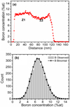 |
Fig. 2 Distribution of Boron for the GILD sample: (a) one-dimensional boron depth distribution calculated by integrating the data of Figure 1 over a cylindrical volume with a radius of 10 nm. (b) Distribution of the boron content (histogram) in sets of 200 atoms located in 30 × 30 × 10 nm3 data slice (position Z2) compared to a binomial distribution. |
3.2 Boron spatial distributions in PLIE samples (3 and 9 at.%at of Boron)
Two samples prepared by PLIE were analyzed by APT. Figure 3 shows their reconstructed volume for a boron concentration of 9 and 3 at.%. In addition to the Ni layer, added as a protective layer against Ga implantation during tip preparation and to the Si oxide on the surface, two regions can be identified: a highly boron doped silicon layer and pure silicon. From these volumes, no precipitates or clusters of boron atoms are not visible (in comparison, for the implantation technique, clusters appear even below the boron solubility limit in silicon, perhaps due to the high density of defects generated [4]). The interface from Si to Si:B is found to be sharp, which should be related to the larger greater diffusion of boron atoms in the liquid layer than in the solid material, leading to a box-like doping profile. In all cases, this sharp interface and the high B concentration indicate a metastable state probably due to the high rate speed of recrystallization by epitaxy on silicon.
From these reconstructions, one dimensional boron depth distributions were calculated by a radial integration over a cylindrical region of 10 nm diameter perpendicular to the Si/Si:B interface. Figure 4a shows the depth profiles of these samples; the B concentration is constant and equal to 3 at.% and 9 at.% at depths of 100 nm and 20 nm, respectively. In this case, two laser annealing conditions of pre-implanted silicon were used in order to obtain two boron concentrations over two different melting depths.
Figure 4a shows that the boron concentration measured by APT agrees with the SIMS profile obtained by isotopic comparison [28]. In principle, it is difficult to quantify high concentrations above 1 at.% by SIMS, since in this concentration range, the dilute regime should no longer be valid. The good agreement between the APT and SIMS curves confirms on one hand the accuracy of the isotopic comparison method used to calibrate SIMS measurements for this alloy concentration range. On the other hand, an accurate quantification of boron in heavily doped silicon can be obtained by APT without calibration. This was unexpected given the reported disagreement between APT and SIMS for the weakly boron-doped Si used in microelectronics.
Figure 4b shows an example of the distribution obtained with a 200 atoms by sets for sample of at 9 at.% B. Similar to the sample obtained by GILD, and the binomial distributions provide good significance values (p-value = 0.5 for both concentration) and match the boron observed distribution leading to the conclusion of a random distribution. The precipitate/clusters procedures were also applied, but no clusters could be detected. A percentage of only 0.09% (respectively 0.03%) of B2 dimers could be detected in the film annealed for 29 ns (rep. 67 ns).
The same results were obtained for GILD and PLIE samples with the same boron concentration of 9 at.%. Finally, the only difference between GILD and PLIE samples is the thickness of the boron-doped silicon, 20 nm for PLIE and 90 nm for GILD. This difference may explain the different values of the transition temperature ‘Tc’ obtained for the two types of techniques. In fact, Kawarada et al. [29] have recently reported that Tc decreases by about 50% as the thickness decreases from 100 nm to 30 nm in B-doped diamond. We have to balance this statement since additional randomness is effectively introduced by the fact that only about a third of the atoms are detected.
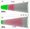 |
Fig. 3 Reconstruction of two volumes in heavily boron-doped silicon epilayers (prepared by PLIE) analyzed by APT. Each point corresponds to an atom. (a) 9 at.% of boron in doped silicon layer and (b) 3 at.% .of boron in doped silicon layer. |
 |
Fig. 4 Boron distribution for PLIE samples: (a) one-dimensional boron depth distribution calculated by integrating the data of Figure 3 over a 10 nm radius cylindrical from the two volumes of Figure 3 and boron depth measured by secondary ion mass spectrometry (SIMS) for 3 at.% of B. (b) Example of distribution of the boron content (histogram) in sets of 200 atoms located in a 30 × 30 × 10 nm3 data slice of 9 at.% boron compared to a binomial distribution. |
3.3 Evaporation field
The evaporation of silicon is expected to be dominated by a thermally assisted process [30]. Indeed, in laserassisted APT experiments, the field evaporation is triggered by the local and transient increase in the temperature of the tip apex. From a theoretical model for the field evaporation of boron in a pure B sample [31], the evaporation field of boron (FB) was estimated to be higher than that the evaporation field of boron (FB) is higher than the evaporation field of silicon (FSi). However, the dependence of the evaporation field of Si:B-alloys on the B concentration is still unknown. To overcome this lack of knowledge, two methods based on our APT measurements are proposed to evaluate the effect of boron composition on the evaporation field. These methods are respectively related to the change in either the applied voltage and to the charge state ratio of Si as function of material composition (Si or Si:B).
3.3.1 Method based on the applied voltage
The evaporation field can be approximated by the electric field F at the surface of the tip. This electric field is now related to the voltage V and the radius of curvature R by the following classical formula [32]: (1)where β, the field factor, is constant and depends on the geometry of the chamber, the distance to the local electrode, etc. Thus if the radius is known, it is possible to have access to the evaporation field via the voltage measurement.
In our samples consisting of a Ni/Si:B/Si structure, boron is homogeneously distributed homogenously in each boron-doped silicon layer with a concentration of either 3 or 9 at.%. Figure 5 shows some examples of the applied voltage used to evaporate these structures.
If the sample had been a made of pure silicon, the voltage would increase linearly with increasing tip radius and shaft size (as shown by the regimes between 0 and 0.7 M ions and 1.3–6 M ions in Fig. 5c). Here, a large increase in the applied voltage V is clearly observed during the analysis of the Si:B layer for each sample. Its amplitude depends on the boron concentration and indicates an increase of the evaporation field. As mentioned above, boron is known to have a higher evaporation field than silicon, so a higher applied voltage is required to evaporate the Si:B alloy. This is indeed what we observe.
We can try to evaluate the evaporation field of the Si:B alloy from the voltage evolution. Few assumptions are required. The tip surface is assumed to be hemispherical and this geometry is maintained during the APT analysis, i.e. the tip radius increases with the shank size and it is not modified by the presence of the Si:B layer. We also chose to use β as suggested in other experiments found in the literature. This value is assumed to be constant for all reconstructions and field evaporation estimates. All these assumptions are not generally true, since in the case of boron delta layers in silicon, for example, it has been shown, that the B layer is retained at the tip surface, leading to a drastic modification of the initial hemispherical surface [33]. In our case, these assumptions are justified because the evaporation field of Si and Ni are similar enough to be considered equal. Since the thickness of the Si:B layer is greater than 20 nm, the tip radius is only modified when Ni and Si:B start to evaporate together due to their different evaporation field. After the Ni layer is completely field evaporated, the large thickness of the Si:B alloy layer allows the tip to reach an equilibrium shape [34,35].
Assuming that the evaporation field of Si and Ni is equal, we can fit the voltage curve between nickel and silicon with the same function (Fig. 5c) taking into account the shank evolution of the tip (VSi∼(ion number)1/3). Then, the tip radius at the center of the Si:B layer could be estimated from the fitted voltage VSi and FSi. At this stage, the applied voltage V is higher than the fitted voltage VSi. The variation of the voltage ratio V/VSi only corresponds to a variation in the evaporation field ratio F/FSi, related to the composition variation.
For each experiment, a portion of the pure silicon substrate was also analyzed by APT. The voltage variation in the Ni and Si regions was fitted with an X1/3 function in order to estimate what would have been the voltage variation VSi in the Si:B region assuming the same field FSi. FSi was then been defined as the reference evaporation field of silicon. The fitted voltage VSi allows us to estimate the evolution of the tip radius R during the analysis, which we write as
 (2)
(2)
Finally, from the evolution of the applied voltage V and the radius R with the ion sequence number, equations (1) and (2) were used to estimate the ratio of the evaporation field F/FSi between the Si:B alloy and Si by (3)
Figure 6 shows the obtained field ratio for two PLIE samples (3 and 9 at.%) where there is a homogeneous composition in the boron-doped silicon layer.
(3)
Figure 6 shows the obtained field ratio for two PLIE samples (3 and 9 at.%) where there is a homogeneous composition in the boron-doped silicon layer.
The curves confirm, that the evaporation field in heavily doped silicon is higher than in undoped silicon and, that this increase depends on the boron concentration. The evaporation field is almost constant in heavily doped silicon and in pure silicon. In fact, the F/FSi ratio varies from 1.15 in Si (3 at.% B) to 1.23–1.25 in Si (9 at.%B) at 84 K. As FB∼2FSi from the theoretical model [32], the value of F/FSi should be 1.03 and 1.09 for Si (3 at.%B) and Si (9 at.%B), respectively, if the variation of the evaporation field is linear with B composition. Our estimate shows a strong increase of the evaporation field for Si (3 at.%B) compared to undoped Si, but a smaller variation when going from 3 to 9 at.%.
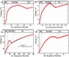 |
Fig. 5 Four curves showing the applied voltages of samples during APT analysis (a) GILD with 9 at.%. (b) GILD with 9 at.% (corresponding to the volume shown in Fig. 1). (c) PLIE with 9 at.% (corresponding to the volume shown in Fig. 2a). (d) PLIE with 3 at.% (corresponding to the volume shown in Fig. 2b). |
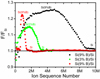 |
Fig. 6 Variation of the ratio of the evaporation field estimated F/FSi from voltage evolution for three Si:B/Si samples at 80 K. |
3.3.2 Method based on the charge states ratio
We also used the model developed by Kingham et al. [36] in order to estimate the variation of the evaporation field between Si:B alloy and pure silicon in the same state. This theoretical model was proposed to relate the evaporation field to the charge state ratio, and to predict the probability of post-ionization. This model of post-ionization can explain both the variation of ion charge state with changing evaporation conditions and the occurrence of highly charged ions. The charge state distribution of field evaporated Si ions was measured as a function of the electric field strength using the pulsed laser atom probe [37]. These measurements were compared with theoretical calculations based on the post-ionization model of field evaporation, and the post-ionization model was validated.
To estimate the field, the ratio of singly- charged Si to doubly-charged Si was therefore measured. Figure 7a shows the fraction of singly charged silicon ( ) as a function of depth from left (Si:B layer) to right (Si substrate) under the same analysis conditions (temperature, evaporation rate and laser energy). A clear variation of the fraction of single charged silicon is observed between undoped Si and boron-doped Si. This variation reflects a change in the evaporation field between undoped Si and boron-doped Si. However, almost the same value is obtained for the different boron concentrations (3 and 9 at.%).
Figure 7b shows the estimated evaporation field with temperature, laser energy and boron concentration from all our experiments. The evaporation field was estimated by comparing the fraction of single charged silicon and the theoretical curve calculated by Kingham. The fraction of single charged silicon is measured from the local mass spectrum in the Si:B alloy and pure silicon. This type of plot highlights the variation of the evaporation field with temperature for the different laser energies and boron concentrations. The presence of 3 and 9 at.% of boron in silicon increases the evaporation field ratio F/F0 by 1.04 at 54 K and 1.06 at 84 K. These results show that the variation of evaporation field of Si:B alloy is not linear with boron concentration. While the evaporation field of undoped silicon decreases with temperature as expected, the evaporation field of Si:B alloy is almost the same for 3 and 9 at.% and it is also independent of temperature.
This unexpected behavior may be due to some limitation of the post-ionization model for Si:B alloy. In fact, since the evaporation field for Si:B alloy is independent of the sample temperature, our results may suggest that the evaporation mechanism of B should include both the tunneling and thermal processes [38]. Evidence for the tunneling mechanism of boron ions during field desorption at temperatures <140 K has already been proposed in the case of a FeB and CoB metallic glass analysis [39]. In reference [40], this tunneling mechanism was associated with a change in the isotope ratio. In GILD samples, the proportion of 10B in the B peak is only 23.3% for single and double charged ions, in disagreement with the relative isotopic abundance. This ratio was verified by SIMS measurements. However, no difference was observed between single and double charged boron ions in the GILD samples. For a tunneling mechanism, and to lesser extent for a post-ionization mechanism, the isotopic ratio change should be opposite for the two charge states. Since this is not the case in our samples, the tunnelling mechanism should not be at the origin of the isotopic change: this could be related to a different chemisorption for the two isotopes for example.
Finally, boron retention phenomena [41] at the tip surface can could explain why the evaporation field of Si:B alloy does not depend on the B concentration in silicon. In fact, during the evaporation of the Si:B layer, boron atoms (high evaporation field) can be retained at the tip surface until an equilibrium shape is reached. The silicon atoms (low evaporation field) have been depleted at the tip surface by preferential evaporation [40]. This could lead to will thus a boron enriched layer at the tip surface. This B-enriched layer may be independent of the boron concentration in heavily doped silicon when the equilibrium is reached, the evaporation field estimated for the Si:B alloy could be then be determined by boron retention.
Comparing the estimation of the evaporation field of silicon-boron alloy with the two methods (applied voltage or charge states), both methods show that the presence of boron in silicon increases the evaporation field. However, the estimated field increases with boron concentration for the voltage method, but it does not change for the charge state method. Since there is much more mechanisms than simple post-ionisation such as tunneling and retention, the post ionization model can be taken with caution in the case of Si:B alloy.
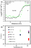 |
Fig. 7 (a) Variation of the single charge state ratio of silicon for two samples Si:B/Si at 80 K and (b) the evaporation field estimated from charge state of silicon for all analyses. |
4 Conclusion
APT was performed to precisely measure the three-dimensional spatial distribution of boron in GILD and PLIE samples. In both types of samples, the boron atoms were found to be randomly distributed in the silicon by means of statistical distribution analysis, and no clusters or precipitates were detected. The random boron distribution combined with the observation of an abrupt Si/Si:B interface demonstrates the feasibility of building innovative devices based on such a GILD- and PLIE-doped silicon. The variation of the evaporation field was studied by considering both the silicon charge state ratio and the variation of the applied voltage during the analysis of the Si:B layer. The evaporation field of Si:B estimated from voltage increases with boron concentration, while it is constant when estimated from charge state ratio. In this case, the evaporation field of Si:B was found to be higher than that of undoped silicon and may not depend on the boron concentration range (3–9at.% of boron) in silicon.
Acknowledgments
This research has been funded by METSA, CNRS-CEA. The authors thank M. Descoins (IM2NP) for technical assistance at FIB and APT technical support. The authors thank also B. Gault (MPIE) is gratefully acknowledged for many interesting and helpful discussions. C. Dubois and G. Prudon are thanked for the SIMS measurements.
Author contribution statement
K. Hoummada: conceptualization, methodology, formal analysis, investigation, writing − original draft, visualization. F. Dahlem: validation, resources, writing − review & editing, formal analysis, investigation. F. Panciera: methodology, formal analysis, investigation, writing. E. Bustarret: conceptualization, methodology, validation, resources, writing − review & editing, project administration, funding acquisition. C. Marcenat: methodology, formal analysis, investigation. D. Débarre : writing − review & editing, project administration, funding acquisition. Y. El Amraoui: writing − review & editing, project administration, funding acquisition. D. Mangelinck: writing − original draft, visualization.
References
- E.C. Jones, E. Ishida, Mater. Sci. Eng., R 24, 1 (1998) [CrossRef] [Google Scholar]
- V. Privitera, Curr. Opin. Solid State Mater. Sci. 6, 55 (2002) [CrossRef] [Google Scholar]
- G. Kerrien, J. Boulmer, D. Débarre et al., Appl. Surf. Sci. 186, 45 (2002) [CrossRef] [Google Scholar]
- E. Bustarret, C. Marcenat, P. Achatz et al., Nature 444, 465 (2006) [CrossRef] [PubMed] [Google Scholar]
- C. Marcenat, J. Kacmarcik, R. Piquerel et al., Phys. Rev. B 81, 020501 (2010) [CrossRef] [Google Scholar]
- F. Dahlem, T. Kociniewski, C. Marcenat et al., Phys. Rev. B 82, 140505 (2010) [CrossRef] [Google Scholar]
- K. Thompson, P.L. Flaitz, P. Ronsheim, D.J. Larson, T.F. Kelly, Science 317, 1370 (2007) [CrossRef] [PubMed] [Google Scholar]
- K. Hoummada, D. Mangelinck, B. Gault, M. Cabié, Scripta Mater. 64, 378 (2011) [CrossRef] [Google Scholar]
- W.K. Yeoh, B. Gault, X.Y. Cui, C. Zhu, M.P. Moody, L. Li, R.K. Zheng, W.X. Li, X.L. Wang, S.X. Dou, C.T. Lin, S.P. Ringer, Phys. Rev. Lett. 106, 247002 (2011) [CrossRef] [PubMed] [Google Scholar]
- A. Cerezo, C.R.M. Grovenor, R.M. Hoyle, G.D.W. Smith, Appl. Phys. Lett. 52, 1020 (1988) [CrossRef] [Google Scholar]
- O. Cojocaru-Mirédin,E. Cadel,F. Vurpillot,D. Mangelinck,D Blavette, Scripta Mater. 60, 285 (2009) [CrossRef] [Google Scholar]
- O. Cojocaru-Mirédin, D. Mangelinck, K. Hoummada, E. Cadel, D. Blavette, C. Perrin-Pellegrino, Scripta Mater. 57, 373 (2007) [CrossRef] [Google Scholar]
- K. Hoummada, I. Blum, D. Mangelinck, A. Portavoce, Appl. Phys. Lett. 96, 261904 (2010) [CrossRef] [Google Scholar]
- P. Ronsheim, P. Flaitz, M. Hatzistergos, C. Molella, K. Thompson, R. Alvis, Appl. Surf. Sci. 255, 1547 (2008) [CrossRef] [Google Scholar]
- K. Thompson, D.J. Larson, T.F. Kelly, Microsc. Microanal. 11, 888 (2005) [Google Scholar]
- P.A. Ronsheim, M. Hatzistergos, J. Vac. Sci. Technol., B 28, 1071 (2010) [Google Scholar]
- G. Kerrien, T. Sarnet, D. Débarre et al., Thin Solid Films 453–454, 106 (2004) [Google Scholar]
- K. Thompson, D. Lawrence, D.J. Larson et al., Ultramicroscopy 107, 131 (2007) [CrossRef] [PubMed] [Google Scholar]
- D.J. Larson, D.T. Foord, A.K. Petford-Long et al., Ultramicroscopy 79, 287 (1999) [CrossRef] [Google Scholar]
- T.F. Kelly, M.K. Miller, Rev. Sci. Instrum. 78, 031101 (2007) [CrossRef] [PubMed] [Google Scholar]
- E. Cadel, F. Vurpillot, R. Larde, S. Duguay, B. Deconihout, J. Appl. Phys. 106, 044908 (2009) [CrossRef] [Google Scholar]
- B. Bourguignon, M. Stoica, B. Dragnea, S. Carrez et al., Surf. Sci. 338, 94 (1995) [CrossRef] [Google Scholar]
- K. Hoummada, F. Dahlem et al., Appl. Phys. Lett. 101, 182602 (2012) [CrossRef] [Google Scholar]
- M.P. Moody, L.T. Stephenson, A. Ceguerra, S.P. Ringer, Microsc. Res. Tech. 71, 542 (2008) [CrossRef] [Google Scholar]
- A. Shariq, T. Al-Kassab, R. Kirchheim, R.B. Schwarz, Ultramicroscopy 107, 773 (2007) [CrossRef] [PubMed] [Google Scholar]
- A. Heinrich, T. Al-Kassab, R. Kirchheim, Mater. Sci. Eng., A 353, 922 (2003) [CrossRef] [Google Scholar]
- D. Vaumousse, A. Cerezo, P.J. Warren, Ultramicroscopy 95, 215 (2003) [CrossRef] [PubMed] [Google Scholar]
- Dubois, G. Prudon, B. Gautier et al., Appl. Surf. Sci. 255, 1377 (2008) [CrossRef] [Google Scholar]
- R. Kanomata, M. Watanabe, S. Kitagoh, R. Nomura, S. Kurihara, Y. Takano, T. Yamaguchi, H. Kawarada, NDNC 2011 International Conference (unpublished) [Google Scholar]
- F. Vurpillot, J. Houard, A. Vella, B. Deconihout, J. Appl. Phys. 42, 125502 (2009) [Google Scholar]
- T.T. Tsong, Surf. Sci. 70, 211 (1978) [CrossRef] [Google Scholar]
- M.K. Miller, A. Cerezo, M.G. Hetherington et al., in Atom Probe Field Ion Microscopy (Clarendon Press, Oxford, 1996), pp. 378–413 [Google Scholar]
- F. Vurpillot, M. Gruber, S. Duguay et al., AIP Conf. Proc. 1173, 175 (2009) [CrossRef] [Google Scholar]
- D.J. Larson,B.P. Geiser,T.J. Prosa,S.S.A. Gerstl,D.A. Reinhard,T.F. Kelly, J. Microsc. 243, 15 (2011) [CrossRef] [Google Scholar]
- D.J. Larson, T.J. Prosa, B.P. Geiser, W.F. Egelhoff Jr, Ultramicroscopy 111, 506 (2011) [CrossRef] [PubMed] [Google Scholar]
- D.R. Kingham, Surf. Sci. 116, 273 (1982) [CrossRef] [Google Scholar]
- G.L. Kellogg, Surf. Sci. 120, 319 (1982) [CrossRef] [Google Scholar]
- A. Menand, D.R. Kingham, J. Phys. D: Appl. Phys. 17, 203 (1984) [CrossRef] [Google Scholar]
- A. Menand, D.R. Kingham, J. Phys. C: Solid State Phys. 18, 4539 (1985) [CrossRef] [Google Scholar]
- A. Goldstein, D. Szostak, Appl. Phys. Lett. 26, 685 (1975) [CrossRef] [Google Scholar]
- D.G. Brandon, Surf. Sci. 5, 137–146 (1966) [CrossRef] [Google Scholar]
Cite this article as: Khalid Hoummada, Franck Dahlem, Federico Panciera, Etienne Bustarret, C. Marcenat, Dominique Débarre, Youssef El Amraoui, and Dominique Mangelinck, Analysis of superconducting silicon epilayers by atom probe tomography: composition and evaporation field, Eur. Phys. J. Appl. Phys. 98, 40 (2023)
All Tables
All Figures
|
Fig. 1 Reconstruction of a 70 × 60 × 180 nm3 volume in heavily boron-doped silicon epilayers (prepared by GILD) analyzed by APT. Each pots corresponds to an atom. |
| In the text | |
|
Fig. 2 Distribution of Boron for the GILD sample: (a) one-dimensional boron depth distribution calculated by integrating the data of Figure 1 over a cylindrical volume with a radius of 10 nm. (b) Distribution of the boron content (histogram) in sets of 200 atoms located in 30 × 30 × 10 nm3 data slice (position Z2) compared to a binomial distribution. |
| In the text | |
|
Fig. 3 Reconstruction of two volumes in heavily boron-doped silicon epilayers (prepared by PLIE) analyzed by APT. Each point corresponds to an atom. (a) 9 at.% of boron in doped silicon layer and (b) 3 at.% .of boron in doped silicon layer. |
| In the text | |
|
Fig. 4 Boron distribution for PLIE samples: (a) one-dimensional boron depth distribution calculated by integrating the data of Figure 3 over a 10 nm radius cylindrical from the two volumes of Figure 3 and boron depth measured by secondary ion mass spectrometry (SIMS) for 3 at.% of B. (b) Example of distribution of the boron content (histogram) in sets of 200 atoms located in a 30 × 30 × 10 nm3 data slice of 9 at.% boron compared to a binomial distribution. |
| In the text | |
|
Fig. 5 Four curves showing the applied voltages of samples during APT analysis (a) GILD with 9 at.%. (b) GILD with 9 at.% (corresponding to the volume shown in Fig. 1). (c) PLIE with 9 at.% (corresponding to the volume shown in Fig. 2a). (d) PLIE with 3 at.% (corresponding to the volume shown in Fig. 2b). |
| In the text | |
|
Fig. 6 Variation of the ratio of the evaporation field estimated F/FSi from voltage evolution for three Si:B/Si samples at 80 K. |
| In the text | |
|
Fig. 7 (a) Variation of the single charge state ratio of silicon for two samples Si:B/Si at 80 K and (b) the evaporation field estimated from charge state of silicon for all analyses. |
| In the text | |
Current usage metrics show cumulative count of Article Views (full-text article views including HTML views, PDF and ePub downloads, according to the available data) and Abstracts Views on Vision4Press platform.
Data correspond to usage on the plateform after 2015. The current usage metrics is available 48-96 hours after online publication and is updated daily on week days.
Initial download of the metrics may take a while.