| Issue |
Eur. Phys. J. Appl. Phys.
Volume 96, Number 3, December 2021
|
|
|---|---|---|
| Article Number | 30301 | |
| Number of page(s) | 9 | |
| Section | Thin Films | |
| DOI | https://doi.org/10.1051/epjap/2021210195 | |
| Published online | 14 December 2021 | |
https://doi.org/10.1051/epjap/2021210195
Regular Article
Nanostructured LaFeO3/Si thin films grown by pulsed laser deposition
1
Université de Toulon, AMU, CNRS, IM2NP, CS 60584, Toulon 83041, France
2
Faculty of Metals Engineering and Industrial Computer Science, AGH University of Science and Technology, al. Mickiewicza 30, 30-059 Cracow, Poland
* e-mail: This email address is being protected from spambots. You need JavaScript enabled to view it.
Received:
28
August
2021
Received in final form:
12
November
2021
Accepted:
22
November
2021
Published online: 14 December 2021
Abstract
The orthorhombic LaFeO3 thin films grown by pulsed laser deposition on silicon showed nano-structuration of their surface and preferential crystallographic exposed facets, depending on the deposition temperature. The LaFeO3 film deposited at 850 °C has two types of grain termination, flat or tip-like, corresponding to two different growth directions, respectively [110] and [200]. However, due to the shape of the termination, the two types of grains expose the same {110} facets. The prepared lanthanum iron oxide films are iron deficient and consequently contains oxygen vacancies, the exact chemical formula being LaFe0.82O3-δ.
© Jędrusik et al., Published by EDP Sciences, 2021
 This is an Open Access article distributed under the terms of the Creative Commons Attribution License (https://creativecommons.org/licenses/by/4.0), which permits unrestricted use, distribution, and reproduction in any medium, provided the original work is properly cited.
1 Introduction
Air quality has grown to be a major health issue. Therefore, actions, through legislations, have been taken to limit the pollutants present in the air, such as CO, NOx, SO2, etc. The tendency seems to be the insertion of always more sensitive gas sensors to monitor the level of pollutants at any moment and anywhere. This is particularly true for the car industry that have then to innovate in a search of cost-effective sensors with high sensitivity, high accuracy and resistant to the heat and the chemical compounds found in the exhaust system. Because they are chemically stable with temperature, perovskite oxides with general stoichiometry ABO3 (A and B being cations of different valences and sizes) are good candidates for that purpose.
Indeed, perovskites are known to be a class of material that produces an extremely large set of physical properties ranging from high-K dielectric to superconductor through catalysis and multiferroic thanks to simple chemical manipulations (exchange of cations, variation in stoichiometry, etc.) [1–3]. Among the abundant number of perovskites, La-based perovskites are of particular interest for their promising applications in catalysis [4,5] and/or in sensing [6,7]. In the case of catalysis, B-site determines the catalytic performance while the main role of the cations in the A-site is to stabilize the structure. Evidently, it is not a clear-cut statement since A-site deficiencies or stoichiometry modification can result in modulations of B-site ions' valence and oxygen vacancies and, as a result, influences the catalytic process [8,9]. The choice of lanthanum in A-site cation, other than its environmental-friendly and biocompatibility characteristics [10], is explained by its slightly larger ionic radius as compared to most of the (3+) rare earth cations. It is believed that this large ionic radius will have for consequence to lower the B-O bond strength and, in return, helps the catalytic process [11]. For instance, LaCrO3 has been studied for its potential propene combustion activity [12] while Sm-doped LaAlO3 for its capability to detect humidity at room temperature [13] and the complex perovskite LaNi1-xCoxO3 for its use as sensing electrode to dopamine, uric acid, and acetaminophen [7].
The most investigated La-based perovskite is certainly lanthanum orthoferrite, LaFeO3, and its derivatives, notably for its NO2 sensing properties [14]. The extended use of iron in La-based perovskite oxides can be explained by its high thermal stability as well as its low price and non-toxicity [15–17]. Lanthanum orthoferrites are mainly elaborated via soft chemistry or standard solid-state reaction to produce powders or films with significant thickness and porosity [14,18]. Although it is well known that film thickness can have a drastic effect on gas sensing properties of the films, only few papers report syntheses of thin LaFeO3 films via physical deposition techniques such as molecular-beam epitaxy (MBE), radio frequency magneton sputtering or pulsed laser deposition (PLD) mainly on crystal substrates [5,19,20].
In that context, the aim of this work is to study the necessary conditions to elaborate valuable LaFeO3 thin films synthesized by Pulsed Laser Deposition (PLD) in presence of oxygen on a (100) silicon crystal with an amorphous 4 nm SiO2 buffer layer. The substrate was selected in anticipation to a possible integration to on-chip microelectronic systems. We will especially focus our attention on the investigation of the influence of process temperature on the morphology and crystallographic structure of the thin films.
2 Methodology
The LaFeO3 (99.9%) target was purchased from the Kurt J. Lesker Company and the (100) oriented Si substrates from the SurfaceNet GmbH (10×10 mm2, average roughness < 0.5 nm). The Pulsed Laser Deposition (PLD) system is equipped with a Nd-YAG (λ = 266 nm) laser and a Neocera chamber. The deposition conditions were an energy density on the target of 2.14 J/cm2, a pulse frequency of 10 Hz and duration of 4 ns and a deposition time fixed at 150 min. X-ray diffraction patterns (XRD) were collected in grazing incidence using a PANalytical EMPYREAN DY 1061 equipped with a Cu Kα tube. The thin films were deposited at three different temperatures (750 °C, 850 °C and 1000 °C) under an oxygen pressure of 40 mTorr. The diffracting phases were identified using the Highscore software. The corresponding cell parameters and crystallites sizes were refined from the XRD patterns with the software MAUD [21]. The penetration depth, defined as the depth at which the intensity of X-rays is divided by e, was calculated using the formula
 with α the incidence angle, 2θ the diffraction angle of the most intense peak of the X-rays diffraction pattern, and μ the linear absorption coefficient [22]. InLens detector and accelerating voltages in the range of 5 kV to 15 kV were employed as Scanning Electron Microscope (SEM) acquisition parameters while Atomic Force Microscopy (AFM) tests were conducted in scan assist mode on surfaces ranging from 100 × 100 nm2 to 2 × 2 μm2 with a scanning frequency of 1 Hz. Transmission Electron Microscopy (TEM) and High-Resolution Electron Microscopy (HREM) images were obtained using a Tecnai G2 ST operating at 200 kV and a JEOL 3010 operated at 300 kV. X-Energy Dispersive Spectroscopy (EDS) analyses were performed with an Si(Li) EDAX detector. More than 20 analyses per sample were acquired, and the K factors for quantification of La and Fe were determined using the LaFeO3 target as standard. The cross sections of the TEM samples were prepared in a conventional way through mechanical grinding, dimpling, followed by ion milling.
3 Results and discussion
3.1 Surface characterization of the LaFeO3 thin films
The surface topology and morphology of the three LaFeO3 thin films were investigated by SEM (Fig. 1) and AFM (Fig. 2). LaFeO3-750 and LaFeO3-850 surfaces present an intriguing nanostructuration, which is absent from the surface of the LaFeO3-1000 layer. This structuration of the surface can be described as nanograins forming either flat regions or bunches of grains with sharp ends (Figs. 1a, 1b, 1d and 1e). Visually, the flat regions are surrounded with the bunches of grains with sharp ends arranged in a spiral groove.
DigitalMicrograph particles analysis functionality was used to gain information regarding the flat area. While there is no particular shape for the regions with grains bunches, the flat regions are usually elongated with a form factor of 0.7 and 0.6 respectively for LaFeO3-750 and LaFeO3-850. No correlation was found in the distribution of the flat areas on the film surface. More informatively, the total flat regions surface shrinks of 13% with the increase of temperature: flat regions in LaFeO3-750 make up for 13% of the image surface while they only account for 6% in LaFeO3-850 images. Also, LaFeO3-750 and LaFeO3-850 SEM images exhibit irregular droplets of nanometric size on top of the layers due to the overheating of the target surface during the deposition process, which can lead to phase explosion phenomena, and the deposition of droplets [23]. Cracks in the layers are only observed in the layer deposited at 750 °C (Fig. 1f). To our knowledge, no such nanostructuration was previously observed in perovskite thin films. SEM pictures of LaFeO3-1000 exhibit a homogeneous covering of shapeless grains with variations of contrast pointing to a significant surface roughness (Figs. 1c and 1g). Low magnification images (not shown here) indicate a certain long-distance structuring that could be a residual ordering of the nanostructures observed at lower temperatures, though this fact should be confirmed by further analyses.
Selected 3D and topographic images obtained via AFM are presented in Figure 2. LaFeO3-750 and LaFeO3-850 surfaces exhibits droplets as observed with SEM (Figs. 2a and 2b). The droplets in the LaFeO3-850 are larger in size and less frequent than the droplet in the LaFeO3-750 due to the influence of the substrate temperature during the elaboration process. Indeed, the increase of substrates' temperature led to the modification of the pressure in the chamber and the mobility of ad-atoms onto the substrate. The higher thermal mobility of ad-atoms onto the thin films surface favored the formation of bigger droplets, hence a reduction of the number of droplets but an enlargement in their diameter. If one discards the droplets, LaFeO3-750 and LaFeO3-850 exhibit similar roughness parameters (Tab. 1). LaFeO3-1000 exhibits a roughness much larger than the lower deposition temperatures: 5 nm for the 1000 °C deposition temperature vs. ∼1.4 nm for the 750 and 850 °C. This confirms the large roughness projected from SEM images for the LaFeO3-1000.
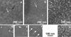 |
Fig. 1 LaFeO3 thin films surfaces observed by SEM: with a x30k magnification (a) LaFeO3-750, (b) LaFeO3-850, (c) LaFeO3-1000; with a x50k magnification: (d) sharp termination grains in LaFeO3-750 (e.g. white arrow in image (a)), (e) flat region in LaFeO3-750 (e.g. black arrow in image (a)), (f) image of LaFeO3-750 showing a crack (pointed out with white arrows), (g) LaFeO3-1000. As an example, the arrow in the image (b) points out to a droplet, i.e. elaboration artifacts. |
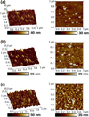 |
Fig. 2 LaFeO3 surfaces observed by AFM a) LaFeO3-750, b) LaFeO3-850 and c) LaFeO3-1000. |
Roughness parameters resulting from AFM analyses of LaFeO3 samples. Measurements were carried out on droplet-free areas.
3.2 Crystallographic structure of the LaFeO3 thin films
The LaFeO3 crystallographic structure is an orthorhombic deformation of the well-known cubic perovskite cell, linked to the tilting of FeO6 octahedra around the axes of the cubic cell and leading to a doubling of the cell parameter along one axis (see Fig. 3). Two settings are used in literature to describe the orthorhombic space group n° 62 of LaFeO3, namely Pbnm and Pnma. We choose the former, for which c is the long axis of the unit cell. The cell parameters are then a = 5.552 Å, b = 5.563 Å, c = 7.843 Å [24]. For the Pbnm setting, the crystallographic relationship between the archetype cubic cell and the orthorhombic one are: (1)
(1)
The Miller indices in the orthorhombic and the cubic descriptions are linked by the following relations: (2)
(2)
The atomic coordinates in the Pbnm setting are given in Table 2 [24].
The XRD patterns from the different thin films, obtained with a grazing incidence angle of 1°, are presented in Figure 4. The corresponding depth of penetration of the X-rays in the LaFeO3 layers is 89 nm. For the three temperatures, only the diffraction peaks corresponding to orthorhombic LaFeO3 were collected, indicating single phased thin films. The XDR patterns of LaFeO3 −750 and −850 seems identical, with 7 peaks that can also be indexed in the archetypal cubic perovskite structure. In fact, with a tolerance factor of 0.89, LaFeO3 is nearly cubic [25]. The XDR pattern of LaFeO3-1000 also exhibits peaks that can only be indexed in the orthorhombic phase. However, this is not linked to an increase of the orthorhombicity of the LaFeO3 structure, as can be seen from the following refinement results. The XRD patterns were refined using the software Material Analysis Using Diffraction MAUD version 2.064 [26]. Starting from CIF file n° 1526450 (Crystallographic Open Database), cell parameters, atomic positions, size, and strain of the crystallites were obtained [27]. The background was fitted with a 5th order polynomial function and the peaks with pseudo-Voigt functions. Errors on cell parameters are 3 × 10⁻³ Å on a and b and 5 × 10⁻³ Å on c. The crystallite size is given with an error of 5 nm and strain with an error of 2 × 10⁻⁴. Results are summarized in Table 3.
Within the errors, all samples exhibit crystallites with similar grain size and strain. A temperature of 1000 °C favors the crystallite growth. The orthorhombic distortion is more pronounced in LaFeO3-850 than in the two other samples. Indeed, the orthorhombic distortion in perovskites can be characterized by the values of  and
and  (in the Pbnm settings). In a plot (
 ,
,  ), with (1,1) being the origin, the polar coordinates of one point gives the magnitude of the orthorhombic distortion, and the deviation from the tetragonal distortion [28]. In Figure 5 we plotted the values obtained in this work and values found in literature. The latter are concentrated around (1,1), thus with a weak orthorhombic distortion and a weak deviation from a tetragonal distortion.
From Figure 5, one can deduce that the LaFeO3 film grown at 1000 °C has the crystallographic orthorhombic structure the nearest from the bulk, and close to those obtained from literature. On the contrary, the structure of the films grown at 850 °C and 750 °C are significantly more distorted than the structures reported in literature. More information on the structure can be obtained from the bond lengths and angles, which were deduced from the refined atomic positions. The latter were obtained with an error of 10−3 for La positions, and an error that varied from 4 × 10⁻³ to 10−2 for oxygen positions. Refined atomic positions, bond lengths and angles are reported Tables 4 and 5.
Compared to Fe-O bond lengths in the LaFeO3 structure reported in the CIF file n° 1526450 [24], the FeO6 octahedra are not deformed for LaFeO3-1000 but are much deformed in case of LaFeO3-750 and LaFeO3-850, with two shortened bond lengths and two stretched bond lengths in the equatorial plane (Fe-O2 bonds) (see Tab. 5). The bond length from Fe to the two-end standing O1 oxygens is only significantly bigger than the reference value for the structure of LaFeO3-850. When looking at the O–Fe–O angles (equal to 90° is the ideal cubic perovskite structure), one can see that the angles in the equatorial plane of the octahedra are the same that in literature, but the angles between the top O1 ions and O2 oxygens in the equatorial plane varies from one sample to another. The distortions in the LaFeO3 thin films can be linked to their chemical composition, which was explored by EDS. A statistical study of the chemical composition was performed for all samples (see Tab. 6). Due to the microstructural particularity of the thin film grown at 1000 °C (appearance of a silicate phase, see TEM results), the EDS analyses were performed on the upper half part of the thin film cross sections, thus avoiding the region near the substrate. The mean composition is the same for the 3 thin films, with a deficiency in Fe. However, the films LaFeO3-750 and LaFeO3-1000 are not homogeneous in composition; we observed different compositions with extremal La/Fe values being 50%/50% and 58%/42%, hence the huge standard deviations. On the contrary, the thin film grown at 850 °C is very homogeneous in composition.
The distortions in the FeO6 octahedra, and hence the global orthorhombic distortion deduced from X-rays diffraction in thin films LaFeO3 can be correlated to the non-stoichiometry of the thin films and their chemical homogeneity. Although the mean composition of the films is the same, LaFeO3-750 and LaFeO3-1000 contains grains with the stoichiometric composition and grains with non-stoichiometric compositions. The contribution to the XRD patterns of the stoichiometric grains shifts the orthorhombicity to values near those of literature for LaFeO3. On the contrary, LaFeO3-850 is very homogeneous (and non-stoichiometric); the orthorhombicity deduced from XRD is consequently more important.
LaFeO3 thin films with an Fe deficiency are not common and we found only one recent reference in literature about La1-yFe1-xO3-δ [34]. The non-stoichiometry of the PLD films could originate in the imposed oxygen partial pressure (40 mTorr) in the PLD chamber during the deposition process [35] or/and in the difference of evaporation rate and speed of the various species vaporized by the laser beam [36]. Charge neutrality in off stoichiometry perovskite can be counterbalanced by oxygen vacancies or reduction of the cation in B site. Reduction of Fe3+ into Fe4+ would reduce the lattice parameter due to a decrease in ion radius [37]. The fact that the volume of the cell decreases with increasing temperature speaks for a higher amount of Fe4+ in the LaFeO3-1000 than in the LaFeO3-750. However, the cell volumes of our samples (Tab. 3) are larger than those found in literature, which are around 242 Å3 [24,29,30]. Thus, one can conclude that oxygen vacancies exist in the lanthanum iron oxide thin films deposited in this work, and their formula should be written LaFe0.82O3-δ.
The thin films grown at 850 °C and 1000 °C were studied by transmission electron microscopy. The films grown at 850 °C is about 150 nm thick (see Figs. 6a and 6c) and the grains are clearly columnar, starting from the SiO2 native layer on top of the Si substrate. The grains lateral size varies from 20 nm to 50 nm, in agreement with the mean size of the crystallites determined by X-rays diffraction, indicating the grain are monocrystalline. Two different morphologies of grain termination are observed; flat ended grains and tip ended ones. HREM (see Figs. 6c and 6d) allowed to unravel the crystallographic facets exposed and the growth direction. Flat ended grains grew along the [110] direction and expose (110) planes (Fig. 6c), as tip ended grains grew along the [020] and expose (110) and (–110) planes (Fig. 6d). Thus, despite of two different growth directions, the exposed facets are the same, namely {110}O = {010}C.
The LaFeO3-1000 thin film shows a completely different morphology, as can be seen in Figure 7. The thin film has an average thickness of 130 nm, but no columnar grains are observed (Fig. 7a). Close to the substrate, a layer of La2Si2O7, 20 nm thick was identified (Fig. 7b). The (002) planes of La2Si2O7, with a spacing of 12 Å, are parallel to the substrate and the layer. Formation of rare earth silicates were already observed after high temperature annealing of films deposited on Si substrate [38], or for thin films deposited by PLD at high temperatures [39,40]. Thus, a temperature of the substrate of 1000 °C during deposition favors the diffusion of Si through the SiO2 barrier, leading to the formation of La2Si2O7. On top of this layer, grains of LaFeO3 with lateral widths larger than in samples with a lower temperature deposition, and with no specific growth direction were identified clarifying XRD observations (Fig. 4). Indeed, for the LaFeO3–750 °C and −850 °C, gains are columnar with specific growth directions which limits the crystallographic planes reachable by the grazing incident XRD technique; this results in a limited number of diffraction peaks. On the contrary, for LaFeO3-1000, which has no particular growth direction, the full range of crystallographic planes are reachable resulting in extra peaks as compared to the low temperature samples. The orientation of the La2Si2O7 layer as observed in HRTEM explains why no peak of this structure was observed in the XRD in a grazing incidence configuration.
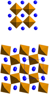 |
Fig. 3 Views along cc of the ideal cubic perovskite structure (top) and along co of the orthorhombic LaFeO3 structure (bottom), showing the tilting of the FeO6 octahedra. |
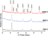 |
Fig. 4 XRD pattern of LaFeO3/Si thin films, indexed in the Pbnm settings. Peaks marked with an * can be indexed in the cubic perovskite phase. The small bump (♢) in the background around 2θ = 56° is due to the (311) planes of the silicon substrate. |
Cell parameters, volume cell, and refinement R factors.
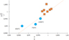 |
Fig. 5 Orthorhombic distortion for the LaFeO3 structure of thin films obtained by PLD at different temperatures (dots). Values obtained from literature (squares) were reported for comparison [20,24,29–33]. The line corresponds to a tetragonal distortion (x = y). |
Refined atomic positions.
Bond lengths and bond angles.
Mean composition for cations obtained by EDS for the LaFeO3 thin films.
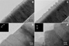 |
Fig. 6 Low magnification (a, c) and HREM (b, d) cross sectional images of the LaFeO3-850 thin film showing the columnar grains and their terminations. The HREM images are presented along with the FFT allowing to identify the exposed facets. |
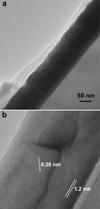 |
Fig. 7 Low magnification (a) and HREM (b) cross sectional images of the LaFeO3-1000 thin film. Grains of LaFeO3, with an imaged reticular distance d(112) = 0.28 nm are on top of a La2Si2O7 layer with (002) planes parallel to the substrate. |
4 Conclusion
Perovskite lanthanum iron oxide thin films were successfully deposited on a SiO2/Si(100) substrate by PLD under vacuum with low oxygen partial pressure at 3 deposition temperatures, 750 °C, 850 °C and 1000 °C. XRD confirmed the orthorhombic structure with Pbnm space group of the films. The main conclusions of this study can be summarized as follows:
-
the films elaborated with deposition temperatures of 750 and 850 °C show uncommon nano-structuration of columnar grains with flat or pointed termination, the mean roughness of the films being around 1.4 nm. Although the two types of grains have different growth directions, the exposed facets belong to the same family of planes {110}O, namely {010}C in the pseudo-cubic description of the material.
-
the film grown at 1000 °C exhibits the largest roughness of the 3 samples, ∼5 nm, but an extra phase, La2Si2O7, at the contact with the substrate was observed indicating the diffusion of Si atoms through the SiO2 buffer layer during the deposition process. The top lanthanum iron oxide layer shows large grains with no specific shape and randomly oriented.
-
x-rays diffraction investigations indicated that all films exhibit orthorhombic distortions as compared to the bulk orthorhombic crystal structure, the 850 °C presenting the larger distortion. These distortions are rationalized in terms of the chemical composition of the films. Chemical analyses revealed an iron deficiency throughout the films leading to the general chemical formula LaFe0.82O3-δ. The reduced distortion for samples deposited at 750 °C and 1000 °C that both exhibit an important dispersion in chemical composition at the nano-scale can be explained by meso-scale investigations of XRD that can only lead to an average distortion information.
In closing, the lanthanum iron oxide thin film elaborated at 850 °C presents interesting characteristics (nanostructuration, free of crack, chemical homogeneity) and will be further studied for its catalytic and sensing properties towards NOx.
Author contribution statement
M. Jedrusik: investigation; Ch. Turquat: investigation, writing −original draft, review and editing; L. Cieniek: investigation; A. Kopia: investigation, supervision; Ch. Leroux: investigation, supervision, writing −original draft, review and editing.
Acknowledgments
This work was done in the general framework of the French-Polish PHC Polonium 40523VD exchange program, with a Ph.D. scholarship of the French embassy in Poland. Authors thank S. Giorgio and D. Chaudanson, from the CiNam, Aix Marseille University, for access to the microscope and support during sessions.
References
- A.S. Bhalla, R. Guo, R. Roy, Mater. Res. Innov. 4, 3 (2000) [CrossRef] [Google Scholar]
- S. Petrović, A. Terlecki-Baričević, Lj. Karanović, P. Kirilov-Stefanov, M. Zdujić, V. Dondur, D. Paneva, I. Mitov, V. Rakić, Appl. Catal. B 79, 186 (2008) [CrossRef] [Google Scholar]
- H. Liu, X. Yang, Ferroelectrics 507, 69 (2017) [CrossRef] [Google Scholar]
- S. Jayapandi, D. Lakshmi, S. Premkumar, P. Packiyaraj, K. Anitha, Mater. Lett. 218, 205 (2018) [CrossRef] [Google Scholar]
- S. Fu, H. Niu, Z. Tao, J. Song, C. Mao, S. Zhang, C. Chen, D. Wang, J. Alloys Compd. 576, 5 (2013) [CrossRef] [Google Scholar]
- K. Wang, J. Song, X. Duan, J. Mu, Y. Wang, New J. Chem. 41, 8554 (2017) [CrossRef] [Google Scholar]
- J. Thomas, P.K. Anitha, T. Thomas, N. Thomas, Microchem. J. 168, 106443 (2021) [CrossRef] [Google Scholar]
- Q. Shen, S. Dong, S. Li, G. Yang, X. Pan, Catalysts 11, 622 (2021) [CrossRef] [Google Scholar]
- X. Li, H. Zhao, J. Liang, Y. Luo, G. Chen, X. Shi, S. Lu, S. Gao, J. Hu, Q. Liu, X. Sun, J. Mater. Chem. A. 9, 6650 (2021) [CrossRef] [Google Scholar]
- B. Liu, J. Nan, X. Zu, X. Zhang, W. Huang, W. Wang, Chemosphere 255, 127010 (2020) [CrossRef] [PubMed] [Google Scholar]
- X.P. Dai, R.J. Li, C.C. Yu, Z.P. Hao, J. Phys. Chem. B. 110, 22525 (2006) [CrossRef] [PubMed] [Google Scholar]
- K. Rida, A. Benabbas, F. Bouremmad, M.A. Peña, E. Sastre, A. Martínez-Arias, Appl. Catal. A 327, 173 (2007) [CrossRef] [Google Scholar]
- S. Pratibha, B. Chethan, Y.T. Ravikiran, N. Dhananjaya, V. Jagadeesh Angadi, Sens. Actuators, A 304, 111903 (2020) [CrossRef] [Google Scholar]
- J.W. Yoon, M.L. Grilli, E.D. Bartolomeo, R. Polini, E. Traversa, Sens. Actuators, B 76, 483 (2001) [CrossRef] [Google Scholar]
- P. Xiao, L. Zhong, J. Zhu, J. Hong, J. Li, H. Li, Y. Zhu, Catal. Today 258, 660 (2015) [CrossRef] [Google Scholar]
- X. Yao, J. Liu, W. Wang, AIP Adv. 8, 115222 (2018) [CrossRef] [Google Scholar]
- I. Tan, H. Tanaka, M. Uenishi, K. Kaneko, S. Mitachi, J. Ceram. Soc. Jpn. 113, 71 (2005) [CrossRef] [Google Scholar]
- K. Lee, S. Hajra, M. Sahu, H.J. Kim, J. Alloys Compd. 882, 160634 (2021) [CrossRef] [Google Scholar]
- E. Traversa, S. Matsushima, G. Okada, Y. Sadaoka, Y. Sakai, K. Watanabe, Sens. Actuators, B 25, 661 (1995) [CrossRef] [Google Scholar]
- A. Cyza, A. Kopia, Ł. Cieniek, J. Kusiński, Mater. Today: Proc. 3, 2707 (2016) [CrossRef] [Google Scholar]
- L. Lutterotti, S. Matthies, H. Rudlolf, Newsletter of the Commission on Powder Diffraction. 21 (1999) [Google Scholar]
- S. Wroński, K. Wierzbanowski, A. Baczmański, A. Lodini, C. Braham, W. Seiler, Powder Diffr. 24, S11 (2009) [CrossRef] [Google Scholar]
- K. Yahiaoui, S. Abdelli-Messaci, S. Messaoud Aberkane, A. Kellou, Appl. Phys. A. 122, 963 (2016) [CrossRef] [Google Scholar]
- L. Sangaletti, L.E. Depero, B. Allieri, P. Nunziante, E. Traversa, J. Eur. Ceram. Soc. 21, 719 (2001) [CrossRef] [Google Scholar]
- E. Haye, F. Capon, S. Barrat, P. Boulet, E. André, C. Carteret, S. Bruyere, J. Alloys Compd. 657, 631 (2016) [CrossRef] [Google Scholar]
- M. Ferrari, L. Lutterotti, J. Appl. Phys. 76, 7246 (1994) [CrossRef] [Google Scholar]
- R. Young, The Rietveld Method, International Union of Crystallograhy, Oxford University Press, Oxford, New York (1993) [Google Scholar]
- W. Paszkowicz, J. Piętosa, S.M. Woodley, P.A. Dłużewski, M. Kozłowski, C. Martin, Powder Diffr. 25, 46 (2010) [CrossRef] [Google Scholar]
- C.A.L. Dixon, C.M. Kavanagh, K.S. Knight, W. Kockelmann, F.D. Morrison, P. Lightfoot, J. Solid State Chem. 230, 337 (2015) [CrossRef] [Google Scholar]
- M. Etter, M. Müller, M. Hanfland, R.E. Dinnebier, Acta Crystallogr., Sect. B 70, 452 (2014) [CrossRef] [Google Scholar]
- M.F. Vignolo, S. Duhalde, M. Bormioli, G. Quintana, M. Cervera, J. Tocho, Appl. Surf. Sci. 197–198, 522 (2002) [CrossRef] [Google Scholar]
- M. Capone, C.J. Ridley, N.P. Funnell, M. Guthrie, C.L. Bull, Phys. Status Solidi B 258, 2000413 (2020) [Google Scholar]
- M. Marezio, P.D. Dernier, Mater. Res. Bull. 6, 23 (1971) [CrossRef] [Google Scholar]
- M.D. Scafetta, S.J. May, Phys. Chem. Chem. Phys. 19, 10371 (2017) [CrossRef] [PubMed] [Google Scholar]
- E. Millon, J. Phys. IV France. 11, Pr7 (2001) [Google Scholar]
- D.B. Chrisey, J.S. Horwitz, R.E. Leuchtner, Thin Solid Films 206, 111 (1991) [CrossRef] [Google Scholar]
- O. Wiranwetchayan, S. Promnopas, S. Phadungdhitidhada, A. Phuruangrat, T. Thongtem, P. Singjai, S. Thongtem, Ceram. Int. 45, 4802 (2019) [CrossRef] [Google Scholar]
- L. Kępiński, W. Miśta, J. Okal, M. Drozd, M. Mączka, Solid State Sci. 7, 1300 (2005) [CrossRef] [Google Scholar]
- M. Jedrusik, L. Cieniek, A. Kopia, Ch. Turquat, Ch. Leroux, Arch. Metall. Mater. 65, 793 (2020) [Google Scholar]
- A. Kopia, K. Kowalski, Ch. Leroux, J.R. Gavarri, Vacuum 134, 120 (2016) [CrossRef] [Google Scholar]
Cite this article as: Mateusz Jędrusik, Christian Turquat, Łukasz Cieniek, Agnieszka Kopia, Christine Leroux , Nanostructured LaFeO3/Si thin films grown by pulsed laser deposition, Eur. Phys. J. Appl. Phys. 96, 30301 (2021)
All Tables
Roughness parameters resulting from AFM analyses of LaFeO3 samples. Measurements were carried out on droplet-free areas.
All Figures
|
Fig. 1 LaFeO3 thin films surfaces observed by SEM: with a x30k magnification (a) LaFeO3-750, (b) LaFeO3-850, (c) LaFeO3-1000; with a x50k magnification: (d) sharp termination grains in LaFeO3-750 (e.g. white arrow in image (a)), (e) flat region in LaFeO3-750 (e.g. black arrow in image (a)), (f) image of LaFeO3-750 showing a crack (pointed out with white arrows), (g) LaFeO3-1000. As an example, the arrow in the image (b) points out to a droplet, i.e. elaboration artifacts. |
| In the text | |
|
Fig. 2 LaFeO3 surfaces observed by AFM a) LaFeO3-750, b) LaFeO3-850 and c) LaFeO3-1000. |
| In the text | |
|
Fig. 3 Views along cc of the ideal cubic perovskite structure (top) and along co of the orthorhombic LaFeO3 structure (bottom), showing the tilting of the FeO6 octahedra. |
| In the text | |
|
Fig. 4 XRD pattern of LaFeO3/Si thin films, indexed in the Pbnm settings. Peaks marked with an * can be indexed in the cubic perovskite phase. The small bump (♢) in the background around 2θ = 56° is due to the (311) planes of the silicon substrate. |
| In the text | |
|
Fig. 5 Orthorhombic distortion for the LaFeO3 structure of thin films obtained by PLD at different temperatures (dots). Values obtained from literature (squares) were reported for comparison [20,24,29–33]. The line corresponds to a tetragonal distortion (x = y). |
| In the text | |
|
Fig. 6 Low magnification (a, c) and HREM (b, d) cross sectional images of the LaFeO3-850 thin film showing the columnar grains and their terminations. The HREM images are presented along with the FFT allowing to identify the exposed facets. |
| In the text | |
|
Fig. 7 Low magnification (a) and HREM (b) cross sectional images of the LaFeO3-1000 thin film. Grains of LaFeO3, with an imaged reticular distance d(112) = 0.28 nm are on top of a La2Si2O7 layer with (002) planes parallel to the substrate. |
| In the text | |
Current usage metrics show cumulative count of Article Views (full-text article views including HTML views, PDF and ePub downloads, according to the available data) and Abstracts Views on Vision4Press platform.
Data correspond to usage on the plateform after 2015. The current usage metrics is available 48-96 hours after online publication and is updated daily on week days.
Initial download of the metrics may take a while.