| Issue |
Eur. Phys. J. Appl. Phys.
Volume 100, 2025
Special Issue on ‘Imaging, Diffraction, and Spectroscopy on the micro/nanoscale (EMC 2024)’, edited by Jakob Birkedal Wagner and Randi Holmestad
|
|
|---|---|---|
| Article Number | 23 | |
| Number of page(s) | 8 | |
| DOI | https://doi.org/10.1051/epjap/2025019 | |
| Published online | 21 August 2025 | |
https://doi.org/10.1051/epjap/2025019
Original Article
In-situ liquid phase TEM of trapped nanoparticles: native-state observation and structural characterization
1
National Centre of Nano Fabrication and Characterisation, DTU Nanolab, Technical University of Denmark, Kongens Lyngby, Denmark
2
InsightChips Aps, Kongens Lyngby, Denmark
* e-mail: This email address is being protected from spambots. You need JavaScript enabled to view it.
Received:
11
March
2025
Accepted:
30
June
2025
Published online: 21 August 2025
Abstract
We developed a system to effectively trap nanoparticles suspended in solution, in dedicated suspended nanochannels for in-situ liquid phase transmission electron microscopy (LPTEM) measurements. The system was tested through single particle analysis using scanning TEM energy dispersive X-ray spectroscopy (STEM-EDX). Furthermore, electron diffraction characterization of metallic nanoparticles in solution was performed for the electron pair distribution function (ePDF). Finally, samples of biological origin were imaged in the liquid cell. The EDX data enabled elemental identification at the single particle level, facilitating the deduction of atomic scattering factors used in the ePDF analysis, which revealed bond lengths for Si-N, N-N from the chip, and Pt-Pt from the sample. We discuss the implications of these findings for in-situ studies of various applications of nanoparticles in liquids. The trap chip system will be useful for biological imaging, time-resolved studies, single particle statistics, and alternatives to X-ray experiments, offering new possibilities for probing dynamic processes with particles in liquids using TEM techniques.
Key words: in-situ liquid phase TEM / single particle analysis / metallic nanoparticles / biological samples / STEM-EDX / electron diffraction
© J. Lafer et al., Published by EDP Sciences, 2025
 This is an Open Access article distributed under the terms of the Creative Commons Attribution License https://creativecommons.org/licenses/by/4.0 which permits unrestricted use, distribution, and reproduction in any medium, provided the original work is properly cited.
1 Introduction
Investigating samples in liquid conditions with Transmission Electron Microscopy (TEM) presents significant challenges due to the need to confine liquids, to prevent evaporation in the vacuum of the TEM column [1]. Traditionally, when looking at a sample that originates from a solution, the sample is dried before TEM analysis [2]. Alternatively, cryogenically frozen samples are often used for biological system. Both drying and freezing the sample compromise the ability to observe dynamic processes in liquid environments [3–5]. Beyond dynamics, critical processes occur in liquid environments, and altering these conditions can modify or even destroy the structure of the sample, leading to misinterpretations [6–8]. While liquid phase electron microscopy offers the opportunity to image samples directly in liquids, keeping nanoparticles stationary for imaging has previously required initially drying the sample, or carefully tuning particle-membrane interactions to act as adhesion, making the process prone to inducing artefacts. We present a direct technique for trapping particles in a liquid cell used for in-situ TEM imaging, spectroscopy, and diffraction for nanoscale characterization. The chip used is a monolithic LPTEM chip manufactured from a silicon substrate through standard microfabrication processes [9]. The viewing area of the chip is a 500 μm x 50 μm membrane consisting of two bonded 20 nm thick silicon nitride (Si3N4) films that are structured to encapsulate the liquid in suspended nanochannels. The trapping principle is illustrated in Figure 1a through a schematic of a single channel with a shallow depth trap at the centre of a deeper nanochannel, all of which consist of suspended and bonded Si3N4 thin films. Both the full height of the channels, as well as the height of the trap, is customizable and determined by the microfabrication processes. When the liquid sample is injected into the chip, any specimen in the liquid that are larger than the height of the trap are physically trapped in the deeper region of the nanochannel, while the liquid can pass through the thin trap region reaching the outlet. When the dimension of the specimen is close to the height of the trap region, the trapping of the specimen also occur in the thinner trap region due to bulging of the membrane.
The channel width is <1.6 μm which only leads to slight bulging ∼10 nm / bar pressure of the channel top and bottom membrane, making the traps only slightly larger when ambient pressure is applied. This is unlike traditional chips with larger membranes, that easily bulge several micrometers which severely impacts the contrast and resolution in LPTEM [1]. With this approach, we are able to achieve atomic scale resolution of gold lattice planes with 1.35Å FFT resolution in the image within the deeper nanochannel, as demonstrated in Figure 1c. Here we present a workflow for preparing samples for TEM characterization of both metallic nanoparticles in solution and samples of biological origin without any surface modification. Single particle analysis is demonstrated through the trapping of metallic particles, with Scanning Transmission Electron Microscopy Energy Dispersive X-ray spectroscopy (STEM-EDX) point measurements to determine the atomic composition. Additionally, electron diffraction of nanoparticle agglomerates is applied for electron Pair Distribution Function (ePDF) analysis with elemental information from the EDX measurements. The imaging of biological ferritin with an iron oxide core achieves high contrast, yielding results comparable to cryo-EM, although limited by the TEM resolution rather than sample preparation constraints.
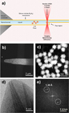 |
Fig. 1 Schematic diagram of a liquid cell with trapping nanochannel for TEM and STEM imaging of monometallic particles stuck in the nanochannels, where lattice fringe resolution in liquid is demonstrated. a) The suspended nanochannels with a controlled height of 100–170 nm, with trap regions ranging from 10-35 nm, are enclosed between two silicon nitride membranes. The nanochannels are filled with a liquid, which can be flowed in or exchanged using an external pump. The e--beam goes through the membrane with the liquid and samples, thus allowing for imaging, spectroscopy, or diffraction measurements. b) HAADF-STEM image of trapped platinum particles in the nanochannels, with 1000 mbar of pressure applied. c) High magnification STEM image of particles in liquid stuck in the trapping region. d) Example of atomic scale resolution imaging of gold nucleation in solution from high electron beam intensity within a filled 60 nm high nanochannel, confined between two 10 nm Si3N4 membranes, captured on a 200 kV TEM. e) FFT of lattice fringe region in (d), showing peaks around 1.35 Å in the Fourier space. |
2 Material and methods
2.1 Ferritin with Iron oxide core
Ferritin from equine spleen in saline solution was obtained from Sigma-Aldrich with a density of 71 mg / mL. The solution was directly used without any modification.
2.2 Metallic nanoparticle mixing
Commercially available nanoparticles (Sigma-Aldrich: silver nanocubes, 75 nm; gold nanoparticles, 50 nm; platinum nanospheres, 30 nm) were mixed into 0.5 mL of Milli-Q water, adding 15, 60, and 60 μL of each solution, respectively. The mixture was then sonicated for 5 min.
2.3 Microscope and EDX acquisition
Both liquid phase and cryo TEM data were collected on an FEI Tecnai T20 G2 with a high tension of 200 kV (λ = 0.02 pm) and a TVIPS XF416 CMOS detector (4096 × 4096 px) was used for imaging. For STEM-EDX an Oxford X-Max 80T SDD X-ray detector was used to capture X-ray signals at an α-tilt of 20° STEM imaging was collected on a High Angle Annular Dark Field (HAADF) detector, and the camera length was set to 150 mm. A selective area diffraction (SAD) aperture with a diameter of 3.8 μm was used to collect diffraction patterns, with a dose rate of 0.15 e−/Å2s. For the cryo-TEM imaging, the same 200 kV Tecnai was used with similar image conditions. An in-situ TEM holder from the company Insight Chips facilitated the flushing of suspended nanoparticle solutions through the trapped chips.
2.4 Preparation of the liquid cell
The ferritin solution was loaded into a chip with a deep nanochannel liquid thickness of ∼110 nm, and shallow 12 nm trap heights, using a dropcasting method [10]. Before filling, Si3N4 membranes sealing the inlets and outlets of the trap chip were punctured using a copper wire. A droplet of aqueous solution (0.2 μL) was placed over each inlet, that is directly connected to an outlet by a bypass microchannel inside the chip. The microchannels also connects to another bypass channel with in/outlets on the other side through the nanochannels across the membrane. Capillary forces draw the liquid into the nanochannels, through the traps and towards to outlets. The complete filling was achieved in seconds, upon droplet contact with the inlet, leading to particle entrapment in the trap channels Figure 1b.
For the metallic nanoparticle solution, a continuous flushing approach was used to maintain pressure in the ∼120 nm high nano-channels, ensuring a sufficient amount of particle flow to the trap and are retained within the nanochannels in front of the 20 nm traps, as seen in Figure 1b. Prior to flushing, the inlets and outlets seals were punctured with a thin copper wire, and the chip was mounted in an Insight Chips TEM flow holder. Initially, Milli-Q water was flushed through both the inlet and outlet to remove potential air bubbles that could obstruct flow. Following this, the mixed metallic nanoparticle solution was connected to one of the inlets and flushed through the chip at a pressure of 1000 mbar. To avoid losing particles via the inflow bypass microchannel because of excessive flow, the outlet was closed, thereby forcing the flow through the nanochannels and traps instead of the bypass channel. The flow through the trap channels made trapped particles pile up preferably towards the traps within the nanochannels (Fig. S6).
3 Results and discussion
3.1 Thickness measurement of the nanochannels
The height of the nanochannels, and thereby the liquid layer, is an important parameter for imaging as well as for a range of different spectroscopy techniques. The thickness of the liquid layer will influence the spatial resolution of the imaging, as well as skew the x-ray results of EDX from absorption in thicker samples, which in turn can influence compositional data [11,12]. For this reason, controlling the thickness of the liquid layer is important for subsequent analysis. The nanochannels were formed by etching the channel design into the silicon substrate using a dry etch process [13]. From measurements acquired by atomic force microscopy (AFM) of a range of channels across the silicon wafer during the fabrication process, the full height of the nanochannels is ∼120 nm, while the thinner parts of the channels have a height of ∼20 nm. However, Zhang et al. (2009) [14] showed that dry etching rates can vary slightly across the wafer, which will result in slight variations of the nanochannels depth, depending on the position of the nanochannel chip on the silicon wafer. For this reason, a method for determining the height of the full channel as well as the thinner trap was implemented.
At the edge of each LPTEM chip membrane are three test-structures, in the form of nanochannels, not connected to the in/outlet bypass channels, so they remain dry during use; the test channels have different heights: one with the height of the trap, one with the height of the full channel minus the height of the trap, and one with the height of the full channel. From TEM images of these test structures and the silicon wedge encapsulating them, it is possible to calculate and estimate the height of the channels [15]. To generate the free-standing Si3N4 membrane, the silicon wafer is etched through by a KOH etch, which will generate side wall along the <111> crystal plane, leaving sloped side walls at an angle of 54.7° (as depicted in Fig. 1). From this slope it is possible to determine the height of the channels through simple trigonometry as the channel height will be protruding the Si wedge in TEM projection images. A schematic principle of the measurement is shown in the supporting information (Fig. S1). From the top view it is possible to calculate the height of the channel (h) using the following expression:
 (1)
(1)
From the approach described above, the height of the thin area of the channel, making up the trap used for the metallic nanoparticle, is 22±3 nm, while the height of the channel minus the trap height was estimated to 96±6 nm. This give a full height of the channel of 129±6 nm.
3.2 Metallic nanoparticles
Controlling nanoparticle formation to obtain a better understanding of their synthesis, is crucial for optimizing their physicochemical properties for specific applications [16]. Studying nanoparticles in solution presents challenges due to the complex interactions between the material, solvent chemicals, and external factors such as pH, temperature, and pressure [17–19]. Furthermore, these particles are typically analyzed either after solvent evaporation to make them adequate for TEM or at high concentrations for X-ray diffraction [20]. In this study, a mix of three metallic nanoparticle solutions with minimal preparation, as described in methods, was flushed through the chip while operating the microscope, to test which size of particles can be flushed in and trapped within the liquid cell. Upon initial observation of the trapped particles, the LPTEM based particle size distribution analysis (Fig. S7), revealed a diameter of 28 ± 6 nm. This is only consistent with the TEM image based size of the 30 nm platinum particles, not the larger silver (75 nm) or gold (50 nm), thereby indicating that only the platinum nanoparticle had entered the traps. An explanation for this could be that the gold and silver particles were too large to enter the nanochannels, due to a double layer or citrate functionalization that will increase the diameter of the particles. From working with the nanochannels, this matches our experience that the diameter of particles should be less than half of the height of the channels to ensure that they are able to enter into the channels. Low-magnification TEM images revealed a mix of dense and dispersed particles trapped in regions in front of the shallow trap, providing an optimal environment for various experimental studies (Fig. S5a). The STEM image in Figure 2a, highlights the contrast coming from the higher scattering cross-section of the metallic nanoparticles. This contrast allows for differentiation between the nanoparticles and the surrounding liquid. The variation in particle distribution allowed for single-particle analysis in low-population areas, where STEM-EDX was employed to examine the individual particle composition. The STEM-EDX data indicated that no silver or gold was present Figure 2b, while the individual particles studied had a clear platinum signature. The STEM-EDX results further support that only the platinum particles had made it into the trap chips In addition to the platinum signal, an unexpected copper signal appeared in the STEM EDX spectra, and a precipitate occurred in the area after the EDX measurement (Fig. S8). SEM EDX measurements on dried particles from each solution did not indicate copper was present in any of the solutions (Fig. S9). Normally no copper signals are present in the chips, but in this case STEM-EDX spectra of water alone in the channel revealed the same contamination (Fig. S10a). We replaced the thin copper wire used to puncture the membrane with a steel needle, and this eliminated the contamination from the spectra (Fig. S10b). The copper wire was oxidized and evidently deposited Cu containing particles into the inlets, which then dissolved upon contact with the liquid, introducing copper ions into the sample. These copper ions underwent a radiolytic reduction due to the high-energy STEM electron beam irradiation, forming metallic copper. We could not identify the copper in the STEM or TEM mode images, as it only occurred after extended irradiation for STEM-EDX acquisition. This illustrates the importance of careful sample preparation as tiny fragments can lead to spurious contaminations in the small volumes of liquid inside such chips. Electron diffraction patterns were collected on particles in the area before the trap, at a position with a high population of particles. The change in position was done to avoid areas that had been subjected to EDX measurements, ensuring that there would be no diffraction signal from irradiation-formed copper particles. This approach mimics powder X-ray diffraction (PXRD) while offering the future possibility for in-situ analysis while changing the environment by flowing in different reagents. Before the diffraction patterns were acquired the tilt of the sample was calibrated using the Si substrate of the chip. A unique feature of the Si-based chip, is that the Si wedge is made from a specifically aligned silicon single crystal. This property serves two purposes: first, it allows precise alignment of the chip to ensure that the membrane is perpendicular to the electron beam, ensuring optimal diffraction geometry where any preferred orientation of particles can be assessed; and second, it enables the calibration of the diffraction pattern with the Si crystal structure, ensuring accurate reciprocal space measurements (Fig. S11). Unlike bulk crystalline materials, nanoparticle samples do not produce a sharp Bragg peak pattern but instead a broader and diffuse ring scattering, because of the polycrystalline nature and random orientation of the particles [21]. This type of scattering, known as total scattering, consists of both elastic and inelastic contributions, captures both long-range and short-range structural information, making it suitable for ePDF analysis [22].
The selected area diffraction (SAD) data collected from a densely populated region is shown in Figure 3, along with the corresponding intensity as a function of the scattering vector (I(Q)) used to obtain the ePDF. For the ePDF a polynomial fit was used to remove the background. The ePDF reveals characteristic peaks of silicon nitride at 1.8 and 2.8 Å, corresponding to previously published bond-lengths [23]. The O-H and O-O bond length from water at 1.8 and 2.8Å, respectively, overlap with the Si3N4 peaks, making it difficult to assess [24]. Future improvements of the ePDF procedure could involve directly subtracting the background signal from a region without particles, and membrane region without liquid, to eliminate silicon nitride and liquid contributions. In addition to the silicon nitride peaks, which overlap with the first platinum interatomic distance at 2.8 Å, small peaks at 4.0 and 4.9 Å are observed, which are characteristic of FCC platinum (Fig. S14). Based on the EDX of the particles, the average electron scattering factor has been calculated as a weighted sum of the individual atomic scattering factors for the membrane and platinum. Then the integrated intensity in Figure 3a is normalized with the electron scattering factors to isolate the total scattering signal from the sample. The rest of the steps in the analysis are demonstrated in Figure S13. While this selection provides a reasonable approximation, further high-Q space refinement could enhance the structural resolution. This could be achieved by increasing exposure times, using higher beam energy, reducing the camera length to access higher Q values, or incorporating mosaic diffraction patterns.
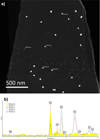 |
Fig. 2 STEM imaging of metallic nanoparticles in a trap, with EDX point spectra showing the elemental compositions. a) STEM image showing the nanoparticles, with the areas corresponding to the spectra marked on the image. b) STEM-EDX point spectra of the particles (lines), with the yellow spectrum aiding as a reference from a region without particles. The characteristic X-ray energies for gold, silver, platinum, and copper are indicated along the spectra. |
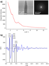 |
Fig. 3 Electron scattering of a selective area of condensed packet platinum particles a) I(Q) of particles in trap channel, from the diffraction pattern obtained with a camera length of 680 mm and an exposure time of 1 second. b) Electron PDF of the platinum particle in the trap chip, a histogram of interatomic distances r. The dampening of oscillations around 12 Å, indicates an individual platinum particle size of 1.2 nm. The characteristic interatomic distances is displayed on the PDF. |
3.3 Ferritin imaging
Ferritin, a 12 nm diameter iron storage protein, plays a crucial role in iron regulation in humans and animals. It consists of a hollow protein shell capable of storing up to 4500 oxidized iron atoms in its 8 nm core [25]. Ferritin is typically imaged dried in TEM or using Cryo-EM, and recently also liquid cells [26,27]. While Cryo-EM enhances resolution, it sacrifices the dynamic properties that liquid cell TEM can provide. With trap chips, ferritin can be trapped and imaged, achieving a resolution similar to that of cryo-EM obtained from the TEM used here (Fig. S4a). The chip used here had a ∼15 nm thin trap region, composed of two 20 nm silicon nitride membranes, and a few ferritin molecules got stuck inside the trapping region with shallow water and higher resolution. In Figure 4, TEM the ferritin remain immobilized, enabling imaging and opening possibilities for single particle analysis of ferritin in liquid phase for comparison to Cryo-EM. The LPTEM size distribution in Figures S3 and 4b reveals a similar size to the cryo TEM characterization, with measured sizes of 8.3 ± 1.4 nm and 7.6 ± 1.3 nm, respectively. The trapping method allows for good contrast imaging from the iron core of ferritin, preserving their native structure and preventing movement, at the level of this TEM's resolution, which has complicated analysis in traditional liquid phase TEM [28]. This method offers a unique way to study the morphology and behavior of ferritin in solution.
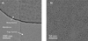 |
Fig. 4 Trapping of Ferritin with iron oxide core. a) Ferritin particles with an iron oxide core are trapped both before and inside the trap. b) The ferritin particles are expected to be 12 nm in diameter, with an 8 nm inner iron oxide core. |
4 Outlook
Using the traps to capture an ensemble of metallic nanoparticles in solution, allows for both crystallographic and structural information to be gathered in the TEM with spectroscopy and diffraction data. Here, diffraction patterns will offer a similar possibility as powder x-ray diffraction, and equivalent atomic pair distribution function analysis could be carried out to find the interatomic distances and unit cell parameters [29–31]. In addition, it could be utilized for phase identification, crystallographic texture analysis, radiolytic beam damage study in liquids, and the detection of strain or defects. The possibility of doing fast experiments with the trap nanochannel gives rise to gathering more data on experimental high entropy alloys (HEA). Here, it could be feasible to collect high-resolution STEM-EDX data to highlight the different metallic components of the synthesis HEAs, together with atomic information from the ePDF [32–34].
Growing crystals large enough to do single-crystal x-ray diffraction (SCXRD) is often a comprehensive and difficult task [35–37]. Once again, the advancement in electron diffraction techniques opens new prospects for carrying out crystallographic studies. 3D ED works on the same principles as SCXRD but with a single crystal, in principle, up to 106 times smaller [38]. One research field that is starting to gain popularity using 3D ED is studying dynamic processes in metal-organic frameworks (MOFs) [39,40]. MOFs are another possible sample to grow or inject in traps. The limitation of these studies is that every dynamic process is generally done, ex-situ, and then usually some kind of treatment to get the sample dry again [41]. This can be overcome by trapping the MOFs and then changing the physical or chemical environment to initiate the structural change.
Trapping catalytic nanoparticles within nanochannels offers a unique, controlled environment for studying catalytic reactions at the nanoscale [42,43]. The ability to introduce reagent liquids and dynamically alter the chemical environment enables real-time observation of reaction processes. This setup allows for direct imaging of reaction sites, capturing changes in both the structure and composition of the catalyst. Additionally, any gases produced during the reaction can be detected using EELS, providing valuable information on reaction intermediates and by-products. Such methodology will further bridged traditional environment TEM with liquid phase electron microscopy to allow in-situ studies into catalytic transformation at high temporal and spatial resolution.
Trapping structures of biological origin provides an alternative to Cryo-EM, though with the added challenge of radiolysis [44]. Better TEM and improved chip designs should one for studies e.g. biomolecular function, stability, and response to external stimuli by real-time tracking of structural and chemical changes, thus enhancing the connection between structural biology and in-situ TEM studies.
5 Conclusion
Trapping particles in LPTEM for imaging and spectroscopic analysis offers unique possibilities to conduct in-situ studies. By utilizing the technique, we preserve the integrity of samples, while achieving single-particle elemental analysis through STEM-EDX and structural characterization using electron diffraction. Selective trapping of nanoparticles in well-defined regions enhances reproducibility, providing precise control over experimental conditions. In addition, this opens up new perspectives for in-situ studies enabling the tracing of real-time nanoparticle dynamics, nucleation and growth and reactions within a controlled liquid environment. By combining LPTEM with time-resolved diffraction and spectroscopic methods, one can track structural changes in real time. Overall, an improvement in methodology for studying dynamic processes at the nanoscale, providing new insights into reaction mechanisms, phase transformation, and interfacial phenomena.
Acknowledgments
The authors acknowledge core facility support at DTU Nano lab and a special thanks to Murat Yesibolati and Paul Kempen from DTU Nano lab for assisting in acquiring high contrast TEM images and cryogenic treatment of ferritin. A special thanks to Hussein Abukar Hussein from Insight Chips for his contribution to chip designs.
Funding
We acknowledge funding from the Novo Nordisk Foundation Grant for Natural and Technical Sciences 2022 No. 0080199, the Innovation Fund Denmark Case 3196-00010B, and the Technical University of Denmark for supporting the study.
Conflicts of interest
Kristian Mølhave and Emil Stilhoff are both founders of Insight Chips used in this work.
Data availability statement
Data is available upon request.
Author contribution statement
K.M and E.S envisioned the project and directed the study. N.B executed the microfabrication of the chips used for the project. M.R acquired data for the ferritin imaging. S.T and J.L acquired the TEM data for the analysis of the metallic nanoparticles. Finally, J.L wrote most of the initial draft with the help from S.T. All authors reviewed and commented on the paper.
Supplementary Material
Fig. 1. Nanochannel thickness estimation a) schematic of the side views of the nanochannel with a height of h, where the distance x is defined. b) Shows a top view of the same principle, which is what will be seen from the TEM image, as shown in c).
Fig. 2. Overview of the trap chip with ferritin a) this design of the trap channels, offers a height variation to trap particles in the narrow region. High contrast comes from the solution in the channels. b) Few particles had made it into the trap region.
Fig. 3. Size distribution of ferritin particles. The size was found from the particles in Figure 4.a, with a mean diameter found was: 8.5 ± 1.4 nm - number of particles: 745.
Fig. 4. Cryo TEM imaging of same ferritin sample as used in the trap chip a) cryo TEM images of ferritin with iron oxide core. b) Particle distribution of (a), with a mean diameter found was: 7.6 ± 1.3 nm - number of particles: 928.
Fig. 5. Metallic nanoparticles in the trap chip a) particles distributed in the trap channel and the dense variation. b) Typical example of one of the traps filled with stuck particles. c) Particle size similarity was early observed in TEM images like this.
Fig. 6. HAADF-STEM images of particles trapped Show flow front to the side channels of particles stuck in a trap, with 1000 mbar pressure applied.
Fig. 7. Particle size distribution Figure S3 c was processed in Fiji [1], with gaussian blur, threshold, fill holes and watershed function to do a particle size analysis. Mean diameter found was: 28 ± 6 nm - number of particles: 2386.
Fig. 8. STEM DF on the area after EDX map Copper signals from the EDX map are displayed with orange dots. Traces of copper are shown all over the background where the liquid solution is present in the chip.
Fig. 9. SEM EDX spectrum of the three metallic solutions All metallic components were analyzed in the SEM to investigate the copper source. The gold, platinum and silver signal was detected in their respective solution, but no copper signal was present.
Fig. 10. STEM-EDX point measurements of the same type of chip, the membranes were punctured differently followed by the same dropcasting of Milli-Q H2O. a) The membrane in the inlets was punctured with a thin copper wire, the same wire as used to puncture the membrane in the experiments conducted in this study. b) A hypodermic needle used to puncture the membrane on the inlets.
Fig. 11. Diffraction pattern of Si (11 ) rotated to ensure perpendicular beam to chip a) diffraction at 0° α tilt. b) Aligned diffraction pattern to the Si wedge at 0.8° α tilt. c) Simulated diffraction pattern of 0° tilt Si (11
 ) from Recipro [2].
Fig. 12. TEM images from the SAD a) particles in trap, a dense area was chosen for diffraction. b) The particles in SAD used for diffraction.
Fig. 13. Steps in ePDF analysis plotted
Fig. 14. Simulated PDF of Pt FCC The simulated diffraction pattern is with similar Q-range as observed in the electron diffraction data. The simulation is done with the python package DebyeSimulator [5].
Access Supplementary MaterialReferences
- F.M. Ross, Opportunities and challenges in liquid cell electron microscopy, Science 350.6267, aaa9886 (2015) [Google Scholar]
- J. Ayache et al., in Sample Preparation Hand-Book for Transmission Electron Microscopy: Techniques, (Springer Science & Business Media, 2010), Vol. 2 [Google Scholar]
- B. Michen et al., Avoiding drying-artifacts in transmission electron microscopy: Characterizing the size and colloidal state of nanoparticles, Sci. Rep. 5, 9793 (2015) [Google Scholar]
- D. Gusnard, R.H. Kirschner, Cell and organelle shrinkage during preparation for scanning electron microscopy: effects of fixation, dehydration and critical point drying, J. Microsc. 110, 51 (1977) [Google Scholar]
- C. Schmidli et al., Miniaturized sample preparation for transmission electron microscopy, J. Vis. Exp.: Jove 137, 57310 (2018) [Google Scholar]
- H. Wu et al., Liquid-phase electron microscopy for soft matter science and biology, Adv. Mater. 32, 2001582 (2020) [Google Scholar]
- L. Li et al., An unusual type of polymorphism in a liquid crystal, Nat. Commun. 9, 714 (2018) [Google Scholar]
- E.S. Grape et al., Breathing metal-organic framework based on flexible inorganic building units, Cryst. Growth Des. 20, 320 (2019) [Google Scholar]
- E. Jensen, A. Burrows, K. Mølhave, Monolithic chip system with a microfluidic channel for in situ electron microscopy of liquids, Microsc. Microanal. 20, 445 (2014) [Google Scholar]
- M.N. Yesibolati et al., Electron inelastic mean free path in water, Nanoscale 12, 20649 (2020) [Google Scholar]
- N. de Jonge et al., Resolution and Aberration Correction in Liquid Cell Transmission Electron Microscopy, Jan. 2019. https://doi.org/10.1038/s41578-018-0071-2 [Google Scholar]
- G. Kothleitner et al., Linking tem analytical spectroscopies for an assumptionless compositional analysis, Microsc. Microanal. 20, 678 (2014). https://doi.org/10.1109/TSM.2007.907627 [Google Scholar]
- S. Lagana et al., Quasi-nanofluidic liquid cell for in situ liquid transmission electron microscopy, in European Microscopy Congress 2016: Proceedings, Wiley Online Library, 2016, pp. 402–403 [Google Scholar]
- Q. Zhang, K. Poolla, C.J. Spanos, Across wafer critical dimension uniformity enhancement through lithography and etch process sequence: Concept, approach, modeling, and experiment, IEEE Trans. Semicond. Manuf. 20, 488 (2007) [Google Scholar]
- M.S. Larsen, Charges and potentials in liquid phase transmission electron microscopy, Ph.D. thesis, 2024 [Google Scholar]
- J.K. Mathiesen et al., Chemical Insights into the Formation of Colloidal Iridium Nanoparticles from In Situ X-ray Total Scattering: Influence of Precursors and Cations on the Reaction Pathway, J. Am. Chem. Soc. 145, 1769 (2023) [Google Scholar]
- J. Quinson et al., Solvent-dependent growth and stabilization mechanisms of surfactant-free colloidal Pt nanoparticles, Chem. Eur. J. 26, 9012 (2020) [Google Scholar]
- P. Lettenmeier et al., Highly active nanosized iridium catalysts: synthesis and operando spectroscopy in a proton exchange membrane electrolyzer, Chem. Sci. 9, 3570 (2018) [Google Scholar]
- T.S. Rodrigues et al., Synthesis of colloidal metal nanocrystals: A comprehensive review on the reductants, Chem. Eur. J. 24, 16944 (2018) [Google Scholar]
- R. Andoulsi, K. Horchani-Naifer, M. Férid, Effect of the preparation route on the structure and microstructure of LaCoO3, Chem. Pap. 68, 608 (2014) [Google Scholar]
- A. Guinier, X-ray diffraction in crystals, in Imperfect Crystals, and Amorphous Bodies. Dorer, 1963 [Google Scholar]
- T.L. Christiansen, S.R. Cooper, K.M.Ø. Jensen, There's no place like realspace: elucidating size-dependent atomic structure of nanomaterials using pair distribution function analysis, Nanoscale Adv. 2, 2234 (2020) [Google Scholar]
- N. Umesaki, N. Hirosaki, K. Hirao, Structural characterization of amorphous silicon nitride by molecular dynamics simulation, J. Non-Cryst. Solids 150, 120 (1992) [Google Scholar]
- M.B. De Kock et al., Determining the radial distribution function of water using electron scattering: A key to solution phase chemistry, J. Chem. Phys. 153, 194504 (2020) [Google Scholar]
- D. Klint, G. Karlsson, J.-O. Bovin, Cryo-TEM Snapshots of Ferritin Adsorbed on Small Zeolite Crystals, Angew. Chem. Int. Ed. 38, 2560 (1999) [Google Scholar]
- L. Houben et al., A mechanism of ferritin crystallization revealed by cryo-STEM tomography, Nature 579, 540 (2020) [Google Scholar]
- R. Dhaoui et al., 3D Visualization of Proteins within Metal-Organic Frameworks via Ferritin- Enabled Electron Microscopy, Adv. Funct. Mater. 34, 2312972 (2024) [Google Scholar]
- M.N. Yesibolati et al., Unhindered Brownian Motion of Individual Nanoparticles in Liquid-Phase Scanning Transmission Electron Microscopy, Nano Lett. 20, 7108 (2020) [Google Scholar]
- Th.E. Weirich et al., Rietveld analysis of electron powder diffraction data from nanocrystalline anatase, TiO2, Ultramicroscopy 81, 263 (2000) [Google Scholar]
- T.E. Gorelik et al., Towards quantitative treatment of electron pair distribution function, Acta Crystallogr. Sect., B: Struct. Sci. Cryst. Eng. Mater. 75, 532 (2019) [Google Scholar]
- S.J.L. Billinge, The rise of the X-ray atomic pair distribution function method: a series of for-tunate events, Philos. Trans. R. Soc. London, Ser. A 377, 20180413 (2019) [Google Scholar]
- E.P. George, D. Raabe, R.O. Ritchie, High-entropy alloys, Nat. Rev. Mater. 4, 515 (2019) [CrossRef] [Google Scholar]
- J.C. Rao et al., Secondary phases in AlxCoCr-FeNi high-entropy alloys: An in-situ TEM heating study and thermodynamic appraisal, Acta Mater. 131, 206 (2017) [Google Scholar]
- X.D. Xu et al., Transmission electron microscopy characterization of dislocation structure in a face-centered cubic high-entropy alloy Al0. 1CoCrFeNi, Acta Mater. 144, 107 (2018) [Google Scholar]
- R.D. Sommer, How to grow crystals for X-ray crystallography, Cryst. Struct. Commun. 80, 337 (2024) [Google Scholar]
- F. Liu, K. Chen, D. Xue, How to fast grow large-size crystals? Innovation 4, 100458 (2023) [Google Scholar]
- K.H. Nam, Real-time monitoring of large-scale crystal growth using batch crystallization for serial crystallography, J. Cryst. Growth 614, 127219 (2023) [Google Scholar]
- L.B. McCusker, Electron diffraction and the hydrogen atom, Science 355, 136 (2017) [Google Scholar]
- Z. Huang et al., 3D electron diffraction as an important technique for structure elucidation of metal-organic frameworks and covalent organic frameworks, Coord. Chem. Rev. 427, 213583 (2021) [Google Scholar]
- Z. Huang, T. Willhammar, X. Zou, Three-dimensional electron diffraction for porous crystalline materials: structural determination and beyond, Chem. Sci. 12, 1206 (2021) [Google Scholar]
- Y. Luo et al., Atomic-scale insights into topotactic transformations in an extra-large-pore zeolite using time-resolved 3D electron diffraction, Nat. Synth. 4, 453 (2025) [Google Scholar]
- B. Altenburger et al., Label-Free Imaging of Catalytic H2O2 Decomposition on Single Colloidal Pt Nanoparticles Using Nanofluidic Scattering Microscopy, ACS Nano 17, 21030 (2023) [Google Scholar]
- S. Levin et al., A nanofluidic device for parallel single nanoparticle catalysis in solution, Nat. Commun. 10, 4426 (2019) [Google Scholar]
- H. Wu et al., Understanding, Mimicking, and Mitigating Radiolytic Damage to Polymers in Liquid Phase Transmission Electron Microscopy, Adv. Mater. 36, 2402987 (2024) [Google Scholar]
Cite this article as: Joakim Lajer, Sofie Tidemand-Lichtenberg, Niccolò Bottauscio, Mervan Ramadan, Emil C.S. Jensen, Kristian S. Mølhave, In-situ liquid phase TEM of trapped nanoparticles: native-state observation and structural characterization, Eur. Phys. J. Appl. Phys. 100, 23 (2025), https://doi.org/10.1051/epjap/2025019
All Figures
|
Fig. 1 Schematic diagram of a liquid cell with trapping nanochannel for TEM and STEM imaging of monometallic particles stuck in the nanochannels, where lattice fringe resolution in liquid is demonstrated. a) The suspended nanochannels with a controlled height of 100–170 nm, with trap regions ranging from 10-35 nm, are enclosed between two silicon nitride membranes. The nanochannels are filled with a liquid, which can be flowed in or exchanged using an external pump. The e--beam goes through the membrane with the liquid and samples, thus allowing for imaging, spectroscopy, or diffraction measurements. b) HAADF-STEM image of trapped platinum particles in the nanochannels, with 1000 mbar of pressure applied. c) High magnification STEM image of particles in liquid stuck in the trapping region. d) Example of atomic scale resolution imaging of gold nucleation in solution from high electron beam intensity within a filled 60 nm high nanochannel, confined between two 10 nm Si3N4 membranes, captured on a 200 kV TEM. e) FFT of lattice fringe region in (d), showing peaks around 1.35 Å in the Fourier space. |
| In the text | |
|
Fig. 2 STEM imaging of metallic nanoparticles in a trap, with EDX point spectra showing the elemental compositions. a) STEM image showing the nanoparticles, with the areas corresponding to the spectra marked on the image. b) STEM-EDX point spectra of the particles (lines), with the yellow spectrum aiding as a reference from a region without particles. The characteristic X-ray energies for gold, silver, platinum, and copper are indicated along the spectra. |
| In the text | |
|
Fig. 3 Electron scattering of a selective area of condensed packet platinum particles a) I(Q) of particles in trap channel, from the diffraction pattern obtained with a camera length of 680 mm and an exposure time of 1 second. b) Electron PDF of the platinum particle in the trap chip, a histogram of interatomic distances r. The dampening of oscillations around 12 Å, indicates an individual platinum particle size of 1.2 nm. The characteristic interatomic distances is displayed on the PDF. |
| In the text | |
|
Fig. 4 Trapping of Ferritin with iron oxide core. a) Ferritin particles with an iron oxide core are trapped both before and inside the trap. b) The ferritin particles are expected to be 12 nm in diameter, with an 8 nm inner iron oxide core. |
| In the text | |
Current usage metrics show cumulative count of Article Views (full-text article views including HTML views, PDF and ePub downloads, according to the available data) and Abstracts Views on Vision4Press platform.
Data correspond to usage on the plateform after 2015. The current usage metrics is available 48-96 hours after online publication and is updated daily on week days.
Initial download of the metrics may take a while.