| Issue |
Eur. Phys. J. Appl. Phys.
Volume 98, 2023
Special Issue on ‘Advances in Renewable Energies, Materials and Technology’, edited by Laurene Tetard, Hamid Oughaddou, Abdelkader Kara, Yannick Dappe and Nabil Rochdi
|
|
|---|---|---|
| Article Number | 29 | |
| Number of page(s) | 7 | |
| Section | Thin Films | |
| DOI | https://doi.org/10.1051/epjap/2023230024 | |
| Published online | 28 April 2023 | |
https://doi.org/10.1051/epjap/2023230024
Regular Article
Mg-Ag-Sb thin films produced by solid-state reactive diffusion
1
Aix-Marseille University ‑ CNRS, IM2NP Faculté des Sciences de Saint-Jérôme case 142, 13397 Marseille, France
2
LASMAR, University of Moulay Ismail, Faculté des Sciences, 11 201 Meknes, Maroc
* e-mail: This email address is being protected from spambots. You need JavaScript enabled to view it.
Received:
28
January
2023
Received in final form:
9
March
2023
Accepted:
15
March
2023
Published online: 28 April 2023
Abstract
α-MgAgSb is a tellurium-free thermoelectric material that exhibits good thermoelectric properties near room temperature. Being made of relatively abundant elements compatible with the complementary metal oxide semiconductor (CMOS) technology, it is considered as a possible solution for the development of high-efficiency thermoelectric devices for heat waste harvesting in microelectronic setups. This study presents a first attempt to investigate the structural properties of MgAgSb thin films prepared by solid-state reactive diffusion. X-ray diffraction (XRD) was used to follow phase formation in thin films, first, in the case of the binary Ag3Sb and Mg3Sb2 compounds, and then, in the case of the ternary system Mg-Ag-Sb. For the later, in situ XRD was used to follow real-time phase formations during the reaction of the bilayerAg3Sb/Mg3Sb2. The results show that the phase α-MgAgSb can be produced by reactive diffusion at the interface of the bilayer. Furthermore, the three phases α, β, and γ are shown to coexist at 360 °C, which can be the result of the thin film geometry (surface and interface effects) or due to a different stoichiometry between these three phases contrasting with usual belief. At temperatures higher than 450 °C, γ-MgAgSb is the only phase stabilized in the film. This study serves as a benchmark for the production of pure α-MgAgSb thermoelectric thin films by reactive diffusion.
© N. Oueldna et al., Published by EDP Sciences, 2023
 This is an Open Access article distributed under the terms of the Creative Commons Attribution License (http://creativecommons.org/licenses/by/4.0), which permits unrestricted use, distribution, and reproduction in any medium, provided the original work is properly cited.
1 Introduction
Since recent years, mobile electronic devices have become essential tools for modern social life. At the same time, their energy consumption has considerably increased due to their growing number of applications. Part of their consumed energy is used for operation, but part of it is lost as dissipated heat in their integrated circuits [1,2]. Thus, the possibility of harvesting this waste heat and to convert it into useful electricity to power up these mobile devices attracts great attention [3–5]. To this aim, thermoelectric generators (TEGs) could be used as ideal energy supply devices, directly converting the temperature difference between the integrated circuit and the external environment into electrical source [6,7].
Indeed, integration in microelectronics setups of TEGs free of scarce and toxic elements maintaining high thermoelectric efficiency close to ambient temperature is considered as an ideal solution for energy harvesting in mobile devices [8]. However, the conversion efficiency of a thermoelectric generator mainly depends on the thermoelectric figure of merit ZT of the thermoelectric material (ZT = S2σT/κ where S, σ, and κ are the Seebeck coefficient, the electrical conductivity, and the thermal conductivity of the material, respectively) [9,10]. In order to possess a high thermoelectric figure of merit, thermoelectric materials should exhibit at the same time a high power factor (PF = S2σ) and low thermal conductivity. Bismuth-telluride based materials are reported so far as the best solutions for near room temperature applications because of unparalleled performances [11,12]. Nevertheless, these compounds are made of relatively rare and toxic elements, which do not match modern industries' environmental and recycling goals. Therefore, exploring and developing bismuth- and tellurium-free thermoelectric materials has become an active effort of current research in the thermoelectric field. MgAgSb-based materials that are composed of abundant and low-level toxicity elements are regarded as promising p-type thermoelectric materials for low-temperature waste heat harvesting [10,13,14]. Furthermore, they are expected to be compatible with the CMOS technology enabling device integration in microelectronic setups.
MgAgSb was first studied for thermoelectric applications in 2012 by Kirkham et al. [15]. Bulk MgAgSb synthesized using conventional methods was shown to exhibit ZT∼ 1 at room temperature, reaching a maximum ZT = 1.4 at 475 K [16–18]. Furthermore, ZT of bulk MgAgSb was shown to be improved by different means, such as multiple-element doping like (Li, Ni, Zn ..) [19–22]. Production and properties of MgAgSb thermoelectric thin films have been significantly less studied, in particular using CMOS-compatible fabrication processes [23–25]. However, thin-film based device technology is more suitable for CMOS integrated harvester applications [26], due to both industrial process compatibility and reduced heat conductivity. In 2020, Oueldna et al. [25] shown that MgAgSb thin films could be successfully produced using CMOS-compatible magnetron sputtering. MgAgSb films were prepared by magnetron sputtering and non-diffusive reaction, and phase transitions were studied in detail in the films by in situ XRD [24]. They recently evidenced that the phase α-MgAgSb is not a stoichiometric compound [24], and that its stoichiometry variations could affect its Seebeck coefficient [23]. Nevertheless, obtaining a bulk material [15–17,27] or a thin film [23–25] containing only the thermoelectric phase α-MgAgSb remains a serious challenge, since Mg-Ag-Sb alloys are easily oxidized and easily form multiphase structures, having a significant impact on thermoelectric properties [25,27].
The present work reports an original method for the growth of MgAgSb thin films based on magnetron sputtering and solid-state reactive diffusion [28] between the two binary phases Ag3Sb and Mg3Sb2, expected to be in equilibrium with the ternary phases [29]. The results offer new prospects for the preparation of high-performance tell urium-free thermoelectric devices.
2 Experimental section
All the films elaborated in this study were deposited on the native oxide of Si(001) substrates using a commercial magnetron sputtering system exhibiting a base pressure of 10−8 Torr. Pure Ag, Mg, and/or Sb targets (99.9999% purity) supplied by CODEX international were sputtered in pure argon atmosphere (99.9999% purity) at 5 rpm substrate holder rotation. A presputtering step was performed on the Ag, Mg, and Sb targets prior to deposition in order to clean the surfaces of the targets of possible contaminants and oxide layers. The deposition fluxes were calibrated according to the thickness measurements by X-ray reflectivity. The native SiO2 layer was used as atomic diffusion barrier, avoiding any intermixing between the deposited film and the Si substrate.
In the case of the Ag3Sb film, Ag and Sb were co-deposited in the correct stoichiometry (75 at% Ag and 25 at% Sb) at room temperature (RT) before non-diffusive reaction [30] performed at 250 °C by ex situ annealing under a vacuum of ∼10−7 Torr. The binary Mg3Sb2 film and the ternary MgAgSb film were grown by solid-state reactive diffusion from the reaction of a Mg/Sb or Ag3Sb/Mg3Sb2 bilayer, respectively. The thickness of each film in the bilayers were adjusted considering the atomic densities of monoatomic films (Mg, Ag, or Sb) to match the stoichiometry of the desired compound (see Tab. A1 for Mg3Sb2 and Tab. A2 for MgAgSb in Appendix). The samples were annealed after deposition in situ in a XRD setup.
All the XRD measurements were performed in the Bragg- Brentano geometry (θ−2θ) in a Panalytical Empyrean diffractometer equipped with a PIXcel detector designed for high-speed data collection, using a Cu K-α source (λKα= 0.154 nm). The samples were loaded in an Anton Paar TTK 600 chamber under vacuum (10‑6 Torr) equipped with a heating stage for in situ annealing. The temperature (T) was increased from 30 °C to 550 °C using 5 °C min‑1 steps and 5 min long XRD acquisitions, which correspond to an average temperature ramp of 0.5 °C min−1.
3 Results and discussion
The goal of the study is to determine if thermoelectric α-MgAgSb thin films can be produced combining magnetron sputtering and solid-state reactive diffusion. This compound being composed of three elements, this first investigation is based on the reaction of two binary phases containing the three elements in the correct proportion adjusting the thickness of the binary layers. Thus, Section 3.1 presents the processing conditions and the heat treatments allowing the two binary compounds Ag3Sb and Mg3Sb2to be formed in the bilayer system, before to present the in situ XRD study of the phase formation sequence during reactive diffusion in the Ag3Sb/Mg3Sb2 bilayer in Section 3.2.
3.1 Formation of Ag3Sb and Mg3Sb2 layers
Figure 1 shows the X-ray diffractogram measured on an Ag0.75Sb0.25 layer after Ag and Sb co-sputtering and annealing at 250 °C for 30 min. The peaks detected at 2θ = 35°, 37°, 39°, 52°,62°, 69°, and 75° respectively correspond to the atomic planes (101), (002), (111), (121), (103), (131) and (212) of the compound Ag3Sb according to the ICDD database [31]. The film is polycrystalline and Ag3Sb is the only compound detected in the film, validating the Ag-Sb stoichiometry reached in the Ag-Sb co-sputtered films (no pure Ag or Sb grains detected).
A similar study was performed aiming at producing Mg3Sb2 thin films by non-diffusive reaction (see Fig. A1 in Appendix). However, despite the optimization of the stoichiometry of Mg and Sb atoms (60 at% Mg and 40at% Sb), a film containing only the phase Mg3Sb2 could not be produced. All the Mg3Sb2 films elaborated by Mg and Sb co-sputtering and non-diffusive reaction were always containing a fraction of the pure Sb phase. Thus, the formation of a Mg3Sb2 film via solid-state reactive diffusion between a pure Mg layer and a pure Sb layer (Mg/Sb bilayer) was also investigated. Figure 2 presents the XRD pattern obtained on the as-deposited Mg/Sb bilayer. Diffraction peaks are observed at 2θ = 24°, 25°, 33°, and 51°, corresponding to the (002), (101), (102), and (004) atomic planes of the compound Mg3Sb2, respectively. The as-deposited film already contains the desired compound, probably formed at the interface of the amorphous Sb and Mg layers (see inset in Fig. 2). One can note that all the diffraction peaks observed for powder samples are not detected. This is usual in the case of thin films, as surfaces and interfaces may support textures different from the random distribution.
In situ XRD was used to study the phase sequence of the Mg/Sb bilayer reaction. Figure 3a shows the temperature-dependent XRD patterns recorded during annealing. The variations of the integrated and normalized intensities of the Mg3Sb2(002) and Sb(012) diffraction peaks are presented in Figure 3b as a function of annealing temperature. Only these two diffraction peaks are shown in Figure 3b for clarity. The intensity of each of these peaks is proportional to the volume of the corresponding phase in the film [25].
Mg3Sb2 is observed to grow during annealing consuming the Sb and Mg layers according to the reaction 3Mg + 2Sb → Mg3Sb2 up to 400 °C. After this temperature, the volume of the phase starts to decrease close to 450 °C, which can be due to surface desorption (Mg is particularly volatile under vacuum [33]). The crystallization of the phase Sb occurs at ∼ 100 °C, as three new peaks appear at that temperature at 2θ = 23°, 28° and 48°, corresponding to the atomic planes (003), (012) and (006) of the Sb phase, respectively. The volume of Sb continuously grows up to the end of the annealing. The Mg layer is never detected, because of its texture, not compatible with the θ−2θ geometry or because it stayed amorphous up to full consumption during Mg3Sb2 growth.
As for non-diffusive reaction, reactive diffusion did allow the formation of a pure Mg3Sb2 film. According to the integration of all the detected diffraction peaks, the volume of Sb corresponds to 8.1% of the film at the end of annealing. It should be noted that, for both Mg3Sb2 samples elaborated either by reactive diffusion or non-diffusive reaction, the most intense crystallographic directions are the same. However, reactive diffusion allows the formation of a Mg3Sb2film containing less than 2% of Sb for temperatures below 400 °C (Fig. 3b).
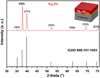 |
Fig. 1 X-ray diffractogram measured at RT on an Ag3Sb film elaborated by non-diffusive reaction compared to the diffraction positions of the Ag3Sb compound [31]. Inset: schematic illustration of the 100 nm thick Ag3Sb/SiO2 sample. |
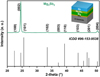 |
Fig. 2 X-ray diffractogram measured at RT on the as-deposited Sb/Mg bilayer compared to the diffraction positions of the Mg3Sb2 compound [32]. Inset: schematic illustration of the Sb/Mg/SiO2 bilayer. |
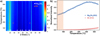 |
Fig. 3 (a) X-ray diffractograms (20° ≤ 2θ ≤ 65°) recorded at different temperatures during in situ annealing of a Mg/Sb bilayer (stars for Mg3Sb2 and diamonds for Sb), (b) normalized intensities of the Mg3Sb2(002) and Sb(012) peaks as a function of temperature. |
3.2 Phase formation sequence in the MgAgSb-thin film
Figure 4a presents the in situ XRD patterns recorded during the annealing of the Ag0.75Sb0.25/Sb/Mg specimen, aiming at MgAgSb thin film growth. In order to match the stoichiometry of the expected Mg1/3Ag1/3Sb1/3 compound, the thicknesses of the deposited layers were determined based on their atomic densities (see Tab. A2 in Appendix).
After deposition, eleven diffraction peaks are observed, which five of them detected at 2θ = 34°, 37°, 39°, 51° and 61° correspond to the (101), (020), (111), (022), and (103) atomic planes of Ag3Sb, respectively. The six other peaks detected at 2θ = 22°, 24°, 25°, 43°, 47° and 50° are respectively attributed to the (100), (002), (101), (103), (201), and (004) atomic planes of Mg3Sb2. This is in agreement with the previous results obtained on the binary systems (Sect. 3.1). Figure 4b presents the variations of the normalized and integrated XRD intensities of the five diffraction peaks Ag3Sb(020), Mg3Sb2(002), α-MgAgSb(110), β-MgAgSb(022), and γ-MgAgSb(022) versus annealing temperature. In the early stage of the phase formation sequence, only the phases Ag3Sb and Mg3Sb2are detected, and the intensity of their diffraction peaks increases with temperature up to a maximum maintained up to a temperature close to 250 °C. This stage corresponds to Figure 5(1).
Around 250 °C, α-MgAgSb forms at the Ag3Sb/Mg3Sb2interface, and grows consuming Mg3Sb2 and Ag3Sb up to T ∼ 320 °C, corresponding to Figure 5(2). This stage corresponds to the decrease of the peak's intensities of Mg3Sb2and Ag3Sb in favor of the peaks of α-MgAgSb in Figure 4b. The diffraction peaks of α-MgAgSb are observed in the diffractogram (Fig. 4a) at the positions 2θ = 13°, 23°, 31°, 39°, 41°, and 46°, and correspond to the (110), (202), (114), (224), (411), and (422) atomic planes of α-MgAgSb phase, respectively. Once the Ag3Sb is fully consumed, α-MgAgSb begins to transform into the phase β, the latter being identified by four diffraction peaks located at 2θ = 12°, 31°, 38°, and 53°, corresponding to the reflections (001), (101), (111), (112), and (004) of β-MgAgSb, respectively. It is interesting to note that β-MgAgSb coexists with Mg3Sb2 at this stage (Fig. 5(3)), as the peak intensity of the phase Mg3Sb2 remains constant in Figure 4b. At T ∼ 360 °C, Mg3Sb2 reacts with the phase α to form of a new phase that corresponds the higher phase γ-MgAgSb, while the phase β continue to grow. New peaks appear located at 2θ = 23°, 38°, 45, 47°, 51°, and 60°, corresponding to the (111), (022), (131), (222), (040), and (133) planes of the phase γ, respectively (Fig. 4a). The intensity of the Mg3Sb2peaks decreases simultaneously with that of the phase α, while the intensity of the diffraction peaks of β and γ increases. At this stage, the four phases Mg3Sb2, α, β, and γ are present in the sample corresponding to Figure 5(4). Mg3Sb2 and α are both consumed after T ∼ 375 °C and the film only contains the phases β-MgAgSb and γ-MgAgSb. β-phase reaches its maximum volume at T ∼ 400 °C, before to be consumed to form the phase γ-MgAgSb corresponding to Figure 5(5). γ-MgAgSb reaches its maximum volume close to T ∼ 450 °C and becomes the only phase detected in the film (Fig. 5(6)). Beyond this temperature, the intensity of the diffraction peaks of γ-MgAgSb reached a plateau as shown in Figure 4b. The phase γ persists until the end of the experiment at T = 550 °C.
These results show that the stoichiometry of the three ternary phases α-MgAgSb, β-MgAgSb, and γ-MgAgSb are different as we previously reported [24]. The complete phase formation sequence for the solid-state reactive diffusion of the Ag3Sb/Mg3Sb2 bilayer is summarized in Figure 5.
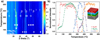 |
Fig. 4 (a) X-ray diffractograms (20° ≤ 2θ ≤ 65°) recorded at different temperatures during in situ annealing from 30 °C to 550 °C, (Mg3Sb2: stars, Ag3Sb: diamonds, α-MgAgSb, β-MgAgSb, and γ-MgAgSb are shown by their symbols). (b) Normalized intensities of the peaks (Ag3Sb(020): diamonds, Mg3Sb2(002): stars, α-MgAgSb(110), β-MgAgSb(022), and γ-MgAgSb(022) as a function of temperature, during in situ annealing. Inset: schematic of the stack: Ag0.75Sb0.25/Sb/Mg/SiO2/Si. |
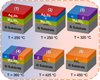 |
Fig. 5 Schematics illustrating the phase formation sequence observed during solid-state reactive diffusion of the Ag3Sb/Mg3Sb2 bilayer. |
4 Conclusion
In this work, anAg3Sb/Mg3Sb2 bilayer was prepared by magnetron sputtering for reactive diffusion, aiming at the growth of a thermoelectric α-MgAgSb film. The results show that it is indeed possible to form the phase α-MgAgSb at the Ag3Sb/Mg3Sb2 interface by reactive diffusion. The reactive diffusion method can be an efficient method to form a pure homogenous α-MgAgSb thin film dedicated to thermoelectric devices to power up electronic and wearable devices. However, the thickness of the Ag3Sb and Mg3Sb2 layers should be adjusted to the real stoichiometry of the phase α-MgAgSb that is different from Mg1/3Ag1/3Sb1/3, which is in turn closer to the stoichiometry of the phase γ-MgAgSb, since a film containing only the phase α could not be obtained, while a pure γ-MgAgSb film was achieved. Furthermore, the phase formation sequence proves that the phase transitions between the phases α, β, and γ are not allotropic, in agreement with our previous reported results. In particular, these three phases are observed to coexist at temperatures above 360 °C.
Acknowledgments
The authors would like to thank Dominique Mangelinck for XRD analysis software. This work was financially supported by CAMPUS FRANCE-PHC TOUBKAL 2018 (French-Morocco bilateral program) Grant Number: TBK/18/65.
Author contribution statement
Nouredine Oueldna: conceptualization, methodology, formal analysis, investigation, writing − original draft, visualization. Alain Portavoce: validation, resources, writing − review & editing, supervision, project administration. Abdelkhalek Kammouni: supervision, funding acquisition. Khalid Hoummada: Conceptualization, Methodology, validation, resources, writing − review & editing, project administration, funding acquisition.
Appendix: A
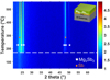 |
Fig. A1 X-ray diffractograms (20° ≤ 2θ ≤ 65°) recorded at different temperatures during in situ annealing of as-deposited Mg0.6Sb0.4 film by non-diffusive reaction (Mg3Sb2: star and Sb: diamond),Inset: schematic illustration of the 100 nm thick Mg0.6Sb0.4/SiO2 sample. |
Summary of the parameters necessary for the calculation of the thickness of the layers: Sb, Mg and Mg3Sb2.
Summary of the parameters necessary for the calculation of the thickness of the layers: Mg3Sb2, Ag3Sb and α-MgAgSb.
References
- W. He et al., Appl Therm Eng. 207, 118176 (2022) [Google Scholar]
- C. Haddad et al., Energy Proc. 50, 1056 (2014) [CrossRef] [Google Scholar]
- A. Tarancón, Nat. Electr. 2, 270 (2019) [CrossRef] [Google Scholar]
- F.K. Shaikh, S. Zeadally, E. Exposito, IEEE Syst. J. 11, 983 (2017) [CrossRef] [Google Scholar]
- S. Chu, A. Majumdar, Nature 488, 294 (2012) [CrossRef] [PubMed] [Google Scholar]
- I. Petsagkourakis et al., Sci. Technol. Adv. Mater. 19, 836 (2018) [CrossRef] [PubMed] [Google Scholar]
- Q.H. Zhang et al., Adv. Eng. Mater. 18, 194 (2016) [CrossRef] [Google Scholar]
- L.E. Bell, Science 321, 1457 (2008) [CrossRef] [PubMed] [Google Scholar]
- G.J. Snyder, E.S. Toberer, Nat. Mater. 7, 105 (2008) [CrossRef] [PubMed] [Google Scholar]
- P. Ying et al., Energ Environ Sci. 15, 2557 (2022) [CrossRef] [Google Scholar]
- H.J. Goldsmid, R.W. Douglas, Br. J. Appl. Phys. 5, 386 (1954) [CrossRef] [Google Scholar]
- H.J. Goldsmid, Materials (Basel) 7, 2577 (2014) [CrossRef] [PubMed] [Google Scholar]
- P.J. Ying et al., Small 18, 2201183 (2022) [CrossRef] [Google Scholar]
- Z.H. Liu et al., Joule. 5, 1196 (2021) [CrossRef] [Google Scholar]
- M.J. Kirkham et al., Phys. Rev. B 85, 144120 (2012) [Google Scholar]
- H.Z. Zhao et al., Nano Energy 7, 97 (2014) [CrossRef] [Google Scholar]
- P.J. Ying et al., Chem Mater. 27, 909 (2015) [CrossRef] [Google Scholar]
- D. Kraemer et al., Energy Environ. Sci. 8, 1299 (2015) [CrossRef] [Google Scholar]
- Z.H. Liu et al., Energy Environ. Sci. 11, 23 (2018) [CrossRef] [Google Scholar]
- Z.H. Liu et al., Nano Energy 31, 194 ( 2017) [CrossRef] [Google Scholar]
- C.Y. Sheng et al., J. Appl. Phys. 119, 195101 (2016) [Google Scholar]
- Z.H. Liu et al., Adv. Energy Mater. 6, 1502269 (2016) [CrossRef] [Google Scholar]
- N. Oueldna et al., J. Alloys Compd. 932, 167692 (2023) [Google Scholar]
- N. Oueldna et al., J. Alloys Compd. 900, 163534 (2022) [Google Scholar]
- N. Oueldna et al., Mater. Lett. 266, 127460 (2020) [Google Scholar]
- A. Portavoce et al., Materialia 14, 100873 (2020) [Google Scholar]
- A. Duparchy et al., J. Mater. Chem. A 10, 21716 (2022) [CrossRef] [Google Scholar]
- E. Assaf et al., Appl. Surf. Sci. 488, 303 (2019) [CrossRef] [Google Scholar]
- B.R.T. Frost, G.V. Raynor, Proc. R. Soc. Lond., Ser. A 203, 132 (1997) [Google Scholar]
- A. Portavoce et al., Appl. Surf. Sci. 437, 336 (2018) [CrossRef] [Google Scholar]
- M.A. Peacock, L. Berry, Univ. Toronto Studies, Geol. Ser. 44, 47 (1940) [Google Scholar]
- E. Zintl, E. Husemann, Zeitsch. Phys. Chem. 21, 138 (1933) [Google Scholar]
- Z. Zhou et al., J. Magn. Alloys. 10, 1719 (2022) [CrossRef] [Google Scholar]
Cite this article as: Nouredine Oueldna, Alain Portavoce, Abdelkhalek Kammouni, and Khalid Hoummada, Mg-Ag-Sb thin films produced by solid-state reactive diffusion, Eur. Phys. J. Appl. Phys. 98, 29 (2023)
All Tables
Summary of the parameters necessary for the calculation of the thickness of the layers: Sb, Mg and Mg3Sb2.
Summary of the parameters necessary for the calculation of the thickness of the layers: Mg3Sb2, Ag3Sb and α-MgAgSb.
All Figures
|
Fig. 1 X-ray diffractogram measured at RT on an Ag3Sb film elaborated by non-diffusive reaction compared to the diffraction positions of the Ag3Sb compound [31]. Inset: schematic illustration of the 100 nm thick Ag3Sb/SiO2 sample. |
| In the text | |
|
Fig. 2 X-ray diffractogram measured at RT on the as-deposited Sb/Mg bilayer compared to the diffraction positions of the Mg3Sb2 compound [32]. Inset: schematic illustration of the Sb/Mg/SiO2 bilayer. |
| In the text | |
|
Fig. 3 (a) X-ray diffractograms (20° ≤ 2θ ≤ 65°) recorded at different temperatures during in situ annealing of a Mg/Sb bilayer (stars for Mg3Sb2 and diamonds for Sb), (b) normalized intensities of the Mg3Sb2(002) and Sb(012) peaks as a function of temperature. |
| In the text | |
|
Fig. 4 (a) X-ray diffractograms (20° ≤ 2θ ≤ 65°) recorded at different temperatures during in situ annealing from 30 °C to 550 °C, (Mg3Sb2: stars, Ag3Sb: diamonds, α-MgAgSb, β-MgAgSb, and γ-MgAgSb are shown by their symbols). (b) Normalized intensities of the peaks (Ag3Sb(020): diamonds, Mg3Sb2(002): stars, α-MgAgSb(110), β-MgAgSb(022), and γ-MgAgSb(022) as a function of temperature, during in situ annealing. Inset: schematic of the stack: Ag0.75Sb0.25/Sb/Mg/SiO2/Si. |
| In the text | |
|
Fig. 5 Schematics illustrating the phase formation sequence observed during solid-state reactive diffusion of the Ag3Sb/Mg3Sb2 bilayer. |
| In the text | |
|
Fig. A1 X-ray diffractograms (20° ≤ 2θ ≤ 65°) recorded at different temperatures during in situ annealing of as-deposited Mg0.6Sb0.4 film by non-diffusive reaction (Mg3Sb2: star and Sb: diamond),Inset: schematic illustration of the 100 nm thick Mg0.6Sb0.4/SiO2 sample. |
| In the text | |
Current usage metrics show cumulative count of Article Views (full-text article views including HTML views, PDF and ePub downloads, according to the available data) and Abstracts Views on Vision4Press platform.
Data correspond to usage on the plateform after 2015. The current usage metrics is available 48-96 hours after online publication and is updated daily on week days.
Initial download of the metrics may take a while.