| Issue |
Eur. Phys. J. Appl. Phys.
Volume 97, 2022
|
|
|---|---|---|
| Article Number | 7 | |
| Number of page(s) | 5 | |
| Section | Imaging, Microscopy and Spectroscopy | |
| DOI | https://doi.org/10.1051/epjap/2022210276 | |
| Published online | 04 February 2022 | |
https://doi.org/10.1051/epjap/2022210276
Regular Article
Visualizing the effects of plasma-generated H atoms in situ in a transmission electron microscope★
1
LPICM, École polytechnique, IP Paris, CNRS UMR7647, 91120 Palaiseau, France
2
LSI, École polytechnique, IP Paris, CEA-DRF-IRAMIS, CNRS UMR7642, 91120 Palaiseau, France
* e-mail: This email address is being protected from spambots. You need JavaScript enabled to view it.
Received:
6
December
2021
Accepted:
3
January
2022
Published online: 4 February 2022
Abstract
The radicals and atoms generated by a plasma have the effect, among others, of changing the surface energies of materials, which allows one to prepare nano-objects that would not stabilise in other conditions. This is the case of the Sn catalysed silicon nanowires (NWs) we present in this paper: without plasma, the liquid Sn at the top of NWs is unstable (because Sn naturally wets the Si) so that no growth is allowed, while in presence of the H atoms generated by the plasma, the balance of surface energies is drastically changed; the Sn droplet stabilises and can be used efficiently by the vapour-liquid-solid (VLS) mechanism of growth. Thus, if one wants to study the growth mechanisms of such NWs in situ in the transmission electron microscope (TEM), one has to adapt a plasma system on the TEM. This is precisely what was done at École polytechnique on the NanoMAX environmental TEM. The paper reports on the plasma effects, on the catalyst and on NW growth, recorded in situ in real time, at atomic resolution. The results are discussed in the light of density functional calculations of bare and hydrogenated Si surface energies.
Supplementary material is available in electronic form at https://www.epjap.org/10.1051/epjap/2022210276
Note to the reader: An error in an affiliation of the first author (Jean Luc Maurice) indicating that he has another affiliation currently was false and was corrected on 13 June 2022
Now at Université Paris-Saclay, Centre de nanosciences et de nanotechnologies, Palaiseau, France
Now at CEA-DAM-DIF, 91297 Arpajon, France
© J.-L. Maurice et al., Published by EDP Sciences, 2022
 This is an Open Access article distributed under the terms of the Creative Commons Attribution License (https://creativecommons.org/licenses/by/4.0), which permits unrestricted use, distribution, and reproduction in any medium, provided the original work is properly cited.
1 Introduction
In plasma-enhanced chemical vapour deposition (PECVD), several species are generated in addition to the parent gas molecules (e.g. SiH4 to deposit Si), including in particular radicals and ions that allow one to perform deposition at lower temperature than with standard CVD (where it is the heat of the substrate that cracks the molecules). Some effects of the plasma are related to the presence of ions and of an electric field, while others are due to the radicals and atoms, like changing the surface energies of the growing materials. This, in turn, allows one to prepare objects or structures that would not stabilise in other conditions. Here, we grow silicon nanowires (SiNWs) in situ via the vapour-liquid-solid (VLS) mechanism [1] using Sn as catalyst [2]. Without plasma, the liquid Sn at the top of NWs is unstable (because Sn surface energy is low compared to that of Si) so that no growth is allowed according to Nebol'sin stability criterion [3]. However, in presence of the H atoms generated by the plasma, the Si surface energies are drastically lowered [4]; the Sn droplet stabilises and can be used by the vapour-liquid-solid (VLS) mechanism of growth [5]. The present study is part of a larger project, the aim of which is to understand how the silicon hexagonal-diamond metastable phase (the 2H polytype, which would have interesting optical properties [6]) can be preferred to the stable one (the cubic 3C polytype) during the growth of Si nanowires. The above mentioned PECVD method, with pure Sn particles replaced by Sn-Cu bimetallic NPs as catalyst [7], is up to now the unique way of obtaining the 2H polytype during growth [8,9].
However, the presence of a plasma under the beam would hardly be compatible with high-resolution TEM. Thus, watching the PECVD growth of such NWs in situ, with atomic resolution, represents a significant challenge. To circumvent that incompatibility, we implemented on the H2 line of our in situ TEM (“NanoMAX”, a modified Thermo Fisher Titan Environmental TEM − ETEM) an electron-cyclotron-resonance plasma source, to remotely generate the H atoms necessary for the growth.
2 Experimental setup
The “NanoMAX” microscope has been developed on the base of a Titan ETEM. It can work at 60, 80 or 300 kV and is equipped with an image Cs-corrector. The experiments reported here were recorded at 300 kV. The changes with respect to the standard ETEM regard: (i) the pumping system, where additional pumps allow one to reach 8×10⁻⁸ mbar as base vacuum, while the differential pumping authorises up to 1 mbar in the sample chamber; (ii) the matter sources, which include effusion sources for molecular beam epitaxy (MBE) [10] and 13 gas lines with three entry ports for CVD; (iii) a radical source using a hot capillary tube for experiments on carbon nanotubes and (iv) the electron cyclotron resonance (ECR) plasma source (Aura-Wave from SAIREM [11]), object of the present paper which can deliver hydrogen, nitrogen or oxygen atoms. To avoid the crossing of the plasma by the beam, we implemented the ECR chamber remotely, on the H2, N2 and O2 gas line of the ETEM, at about 30 cm from the sample, as shown in Figure 1a.
Simulations by SAIREM engineers indicate that there are no ions anymore at such a distance from the plasma source [11]. However, neutrals have a much longer diffusion length. Our results demonstrate that H atoms reach the sample with a significant flux. In the results reported in the following, the plasma power was set to 50 W, unless otherwise mentioned.
The present experiments have been performed at a pressure between 1 and 2 Pa, in pure H2, for the dewetting of the Sn catalyst, and with the addition of SiH4 for the growth of Si NWs. In this case, the gas flows were set to H2: 30 sccm; SiH4: 1.5 sccm (standard cubic cm per min).
To apply the process temperatures, we used a Protochips Fusion sample holder, modified for NanoMAX, where heating takes place thanks to Joule effect in a thin SiC membrane. This membrane includes nine 7-μm holes, on the edge of which we carried out the present observations. Protochips provides a numerical table, specific to each individual membrane, that translates the electrical signal into temperature. The uncertainty of this indication is difficult to assess; we sometimes find differences of several tens of degrees Celsius when we compare the outcome of our in situ MBE or CVD growth experiments with the same experiments carried out in macroscopic reactors. Thus, the present measurements are essentially qualitative. A means of rigorously analysing the temperature of those small devices is in development for future quantitative studies.
Images and movies were recorded using a Gatan US 1000 CCD camera and the Gatan Digital Micrograph plugin for recording movies. The recording frame rate was set to 4 fps (frames per second).
 |
Fig. 1 (a) Schematic and (b) photographs of the ECR plasma system on NanoMAX. |
3 Results and discussion
For our first in situ observations of the effects of the remote ECR plasma, we ignited the plasma while Sn nanoparticles (NPs) deposited on SiC were annealed in situ at 400 °C in H2 at 1 Pa. Let us recall that the Sn melting point being at 232 °C, the Sn was liquid. We recorded the evolution between “Plasma OFF” and “Plasma ON” settings corresponding to switching off and on the supply of hydrogen atoms, the H2 + H pressure remaining equal to 1 Pa, see Figure 2.
As long as no H-atoms are brought to the sample (between 0 and 15 s in Fig. 2a), the Sn NPs are most probably covered by a native oxide that forbids any movement, so that NPs appear stuck to the SiC substrate. As soon as the plasma is ignited, after a very short delay time (<1 s), the particles start to move. The first movements are like breathing, probably corresponding to the reduction of the oxide, then diffusion of whole particles goes on, following a Brownian motion (see evolution between 30 s and 1 min in Fig. 2a and supplementary Material, Video 1). Along their random walk, NPs meet and coalesce (Fig. 2a). The most simple explanation of this behaviour is that the nano-droplets de-wet the SiC substrate; so doing, the surface area of their interface with it strongly decreases (Fig. 2b); this, in turn, drastically weakens their attachment and allows them to diffuse.
When one continues the experiment with the above Sn NPs, by introducing silane, Si nanowires start to grow. After growth has been going on for about 1 h, we started decreasing the plasma power to 40, 30, 20, 10 and, finally, 5 W (“plasma 10 W → 5W”, in Fig. 3). At that low power, the liquid Sn at the top of NWs becomes unstable as the flux of atomic hydrogen desorbing from the Si surfaces starts dominating over the flux of adsorbing hydrogen provided by the ECR plasma source. The Si surface energy increases back to its bare value, making it favourable for Sn to wet the NW walls. Of course, after the catalyst droplet has leaked out along the walls, growth is no longer possible. Reciprocally, it is thus demonstrated that, with the presence of H atoms generated by the plasma, the Si surface energies are drastically lowered; the Sn droplet stabilizes and can be used by the VLS mechanism of growth.
Qualitatively, in absence of hydrogen, Si dangling bonds reconstruct at the surface, distorting the bonds and giving a high surface energy. In the presence of hydrogen, dangling bonds are H-saturated and bond distortion is not necessary anymore to reach an energy minimum; the latter, in turn, is drastically lowered compared to that of the bare case. This decrease can be calculated using density functional theory (DFT) [4,12,13].
In the following, we discuss our experimental observations in the light of the DFT calculations performed by two of the present authors (RB & OHD), in a work that was aimed at understanding the stabilization of the hexagonal diamond metastable phase in Si and Ge nanowires [4]. Technical details on the codes and conditions chosen for those calculations can be found in reference [4]; they include numerous surface planes that are found on the walls of cubic Si NWs, i.e.: {100}, {110}, {111}, {112}, {113}, so that one can build up a credible picture of these walls. Here in Figure 3, {111} planes are visible perpendicular to the growth axis, which is thus a 〈111⟩ axis; the NW wall surfaces are obviously not perfect planes, but must be close to 〈110〉 , {112} (parallel to ?111⟩ or {113} (low-energy plane at 10° from {112}). The energies calculated in the bare and hydrogen-covered cases, are reported in Table 1. One can directly see that, for the three values of the hydrogen excess chemical potential ΔµH 1 displayed in Table 1, hydrogenated surfaces always have an energy significantly lower than that of their bare counterpart. The column ΔµHSkdesorb gives the value of ΔµH for H-desorption from the different surfaces Sk (k = (100) 2 × 1, (110), etc.)2; it indicates that desorption occurs at much lower H-chemical potentials than the lowest shown in Table 1 (–0.4 eV).
However, let us now compare the values in Table 1 to the surface energy of liquid Sn (0.575 Jm−2 or 0.036 eVÅ−2 [3]) − assuming that H atoms do not significantly modify it. Two domains appear: (i) for “high” hydrogen chemical potential (ΔµH = 0 and 0.4 eV), Si facets have a surface energy lower than that of liquid Sn, so that Sn would not wet them, as we qualitatively concluded above; (ii) at “low” hydrogen chemical potential (ΔµH = –0.4 eV) in contrast, most of those facets have surface energies higher that that of liquid Sn, so that the latter would wet them. This indicates in turn that, if hydrogenation forbids Sn wetting indeed at high values the H-chemical potential, it is not sufficient at low values of the latter. In other words, the SiNW walls do not need to be bare to be wetted by Sn. If we get back to our experiment shown in Figure 2, switching the plasma power to 5 W was probably equivalent to decreasing the H-chemical potential below a negative value situated somewhere in between those two domains, i.e. between 0 and −0.4 eV. This also indicates that changing the plasma power can act as a “potentiometer” of the hydrogen chemical potential, which may be used, in turn, to tune Sn wetting of silicon.
In other respects, negative values in Table 1 may appear strange for surface energies, as it means that in such conditions those surfaces are energetically more favourable than no surfaces (uncut bulk): for such H-chemical potentials, hydrogen atoms would tend to break a Si crystal if they were allowed to install themselves in those planes of the crystal with a density which is that of the bond density in the planes. Such a scenario is quite improbable, but submitting surfaces to the indicated H-chemical potential is possible, and would indeed deliver such negative surface energies, making them hardly wettable.
Finally, we have recently found [9] that the addition of Cu to Sn, to make Sn-Cu bi-catalysts, allows one to reduce the size of the liquid nanoparticles below 10 nm, which appears to be a necessary condition for obtaining SiNWs with the hexagonal 2H polytype [4,8,9]. Using this mixed catalyst, we discovered a new growth mechanism, which we called liquid-assisted vapour-solid-solid (LAVSS), where the catalyst is made of liquid Sn(Cu) and solid Cu3Si [7,9]. Thanks to this unique method, we have been able to obtain Sn-Cu-catalysed SiNWs in situ, with 2H regions [14].
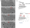 |
Fig. 2 (a) Images taken from Video 1 (available online as supplementary material): TEM plan-views of Sn nanoparticles deposited on the SiC membrane of heating chip, in a hydrogen pressure of 1 Pa and a temperature of 400 °C. Plasma is off at start, then ignited at t = 15 s. (b) Cross-section schematic of the reduction and dewetting processes upon plasma ignition. |
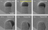 |
Fig. 3 SiNW grown in situ in NanoMAX with one of the Sn catalyst particles shown in Figure 2, at the moment of switching plasma from 10 W (0 s and 8 s, top left) to 5 W (8 s to 16 s). Images extracted from Video 2 (available online as supplementary material). |
4 Conclusion
We have presented a unique piece of equipment that allows one to observe in situ, in the high-resolution TEM, the effect of H-atoms on the shape and behaviour of nano-objects: reduction of Sn-oxide at the surface of Sn nanoparticles, dewetting of these NPs, and growth of Si NWs catalysed by these NPs. The latter, in particular, is quite remarkable as it opens up the way to observing in situ the growth of SiNWs in conditions normally occurring in PECVD reactors [15].
Supplementary Material
Video 1 and Video 2. Access Supplementary Material
Author contribution statement
ÉN & JLM carried out the experimental investigations, helped by IF & WW; JLM & ÉN analysed the data; PB designed and implemented the in situ atomic-hydrogen delivery system; RB and OHD carried out the ab initio calculations; JLM, PRC & MF acquired the Funding; JLM administrated the project and wrote the paper, helped by PRC & OHD. All authors have given approval to the final version of the manuscript.
Acknowledgments
This work was funded by the ANR: TEMPOS-NanoMAX (ANR-10-EQPX-50); HexaNW (ANR-17-CE09-0011). We kindly thank F. Glas and F. Panciera (Université Paris-Saclay, CNRS, Centre de nanosciences et de nanotechnologies) for fruitful discussions. Thanks are also due to the CIMEX for the use of the electron microscopes at École polytechnique.
References
- R.S. Wagner, W.C. Ellis, Appl. Phys. Lett. 4, 89 (1964) [CrossRef] [Google Scholar]
- L. Yu et al., Appl. Phys. Lett. 97, 023107 (2010) [CrossRef] [Google Scholar]
- V.A. Nebol'sin, A.A. Shchetinin, Inorg. Mater. 39, 899 (2003) [CrossRef] [Google Scholar]
- R. Béjaud, O. Hardouin Duparc, Comput. Mater. Sci. 188, 110180 (2021) [CrossRef] [Google Scholar]
- S. Misra et al., J. Phys. D: Appl. Phys. 47, 393001 (2014) [CrossRef] [Google Scholar]
- M. Amato et al., Nano Lett. 16, 5694 (2016) [CrossRef] [PubMed] [Google Scholar]
- É. Ngo et al., J. Phys. Chem. C. 125, 19773 (2021) [CrossRef] [Google Scholar]
- J. Tang et al., Nanoscale 9, 8113 (2017) [CrossRef] [PubMed] [Google Scholar]
- W. Wang et al., ACS Omega 6, 26381 (2021) [CrossRef] [PubMed] [Google Scholar]
- J.-C. Harmand et al., Phys. Rev. Lett. 121, 166101 (2018) [CrossRef] [PubMed] [Google Scholar]
- F. Zoubian, N. Renaut, L. Latrasse, Plasma Res. Express. 3, 025010 (2021) [CrossRef] [Google Scholar]
- J.E. Northrup, Phys. Rev. B. 44, 1419 (1991) [CrossRef] [PubMed] [Google Scholar]
- T. Akiyama et al., Jpn. J. Appl. Phys. 45, L275 (2006) [CrossRef] [Google Scholar]
- É. Ngo, PhD thesis, Institut Polytechnique de Paris, 2021 [Google Scholar]
- J.-L. Maurice et al., Microsc. Microanal. 27, 25 (2021) [CrossRef] [Google Scholar]
The hydrogen excess chemical potential, ΔµH, is defined as follows: ΔµH = µH − µH/SiH4, where µH is the actual hydrogen chemical potential and µH/SiH4 is the cohesive energy for a hydrogen atom in a SiH4 molecule vs the cohesive energy of a Si crystal; ΔµH = 0 corresponds to an energy formation of 0 for SiH4 at the surface of crystalline Si, see details in reference [4].
A bare surface is more stable than its hydrogenated counterpart for ΔµH < ΔµHSkdesorb, see details in reference [4].
“Shuffle” and “glide” refer to the two ways of cutting along {111} planes, well known in plasticity, leaving either a single (“shuffle”) or double (“glide”) dangling bond per surface unit cell.
Cite this article as: Jean-Luc Maurice, Pavel Bulkin, Éric Ngo, Weixi Wang, Martin Foldyna, Ileana Florea, Pere Roca i Cabarrocas, Romuald Béjaud, Olivier Hardouin Duparc, Visualizing the effects of plasma-generated H atoms in situ in a transmission electron microscope, Eur. Phys. J. Appl. Phys. 97, 7 (2022)
All Tables
All Figures
|
Fig. 1 (a) Schematic and (b) photographs of the ECR plasma system on NanoMAX. |
| In the text | |
|
Fig. 2 (a) Images taken from Video 1 (available online as supplementary material): TEM plan-views of Sn nanoparticles deposited on the SiC membrane of heating chip, in a hydrogen pressure of 1 Pa and a temperature of 400 °C. Plasma is off at start, then ignited at t = 15 s. (b) Cross-section schematic of the reduction and dewetting processes upon plasma ignition. |
| In the text | |
|
Fig. 3 SiNW grown in situ in NanoMAX with one of the Sn catalyst particles shown in Figure 2, at the moment of switching plasma from 10 W (0 s and 8 s, top left) to 5 W (8 s to 16 s). Images extracted from Video 2 (available online as supplementary material). |
| In the text | |
Current usage metrics show cumulative count of Article Views (full-text article views including HTML views, PDF and ePub downloads, according to the available data) and Abstracts Views on Vision4Press platform.
Data correspond to usage on the plateform after 2015. The current usage metrics is available 48-96 hours after online publication and is updated daily on week days.
Initial download of the metrics may take a while.