| Issue |
Eur. Phys. J. Appl. Phys.
Volume 94, Number 1, April 2021
|
|
|---|---|---|
| Article Number | 10101 | |
| Number of page(s) | 7 | |
| Section | Semiconductors and Devices | |
| DOI | https://doi.org/10.1051/epjap/2021210015 | |
| Published online | 12 April 2021 | |
https://doi.org/10.1051/epjap/2021210015
Regular Article
Nickel and gold identification in p-type silicon through TDLS: a modeling study
Aix Marseille University, Université de Toulon, CNRS, IM2NP, Marseille 13397, France
* e-mail: This email address is being protected from spambots. You need JavaScript enabled to view it.
Received:
18
January
2021
Accepted:
11
March
2021
Published online: 12 April 2021
Abstract
In Silicon, impurities introduce recombination centers and degrade the minority carrier lifetime. It is therefore important to identify the nature of these impurities through their characteristics: the capture cross section σ and the defect level Et. For this purpose, a study of the bulk lifetime of minority carriers can be carried out. The temperature dependence of the lifetime based on the Shockley-Read-Hall (SRH) statistic and related to recombination through defects is studied. Nickel and gold in p-type Si have been selected for the SRH lifetime modeling. The objective of the analysis is to carry out a study to evaluate gold and nickel identification prior to temperature-dependent lifetime measurements using the microwave phase-shift (μW-PS) technique. The μW-PS is derived from the PCD technique and is sensitive to lower impurity concentrations. It has been shown that both gold and nickel can be unambiguously identified from the calculated TDLS curves.
Note to the reader: Further to the publication of an erratum, the citation of the article was modified on 19 July 2021.
© S. Dehili et al. published by EDP Sciences, 2021
 This is an Open Access article distributed under the terms of the Creative Commons Attribution License (https://creativecommons.org/licenses/by/4.0), which permits unrestricted use, distribution, and reproduction in any medium, provided the original work is properly cited.
1 Introduction
In 2019, 27% of the global electricity generation was ensured by the use of renewable energies [1] and the energy mix is constantly evolving. This change is driven by environmental issues, climate change policies, economical and geopolitical motivations for energy independence. The penetration rate of solar energy remains low, it represents around 3% of global power output despite its high potential. Major drop in costs of solar equipment should, however, allow a strong growth of PV. The international energy agency (IEA) forecasts a solar photovoltaic power generation as high as 16% in 2050.
Due to its high availability, well-established technology showing high conversion efficiency and good durability, silicon dominates the photovoltaic market. Crystalline silicon wafers have a share up to 95% of the worldwide market [2]. Despite the high-efficiency level of this technology, silicon ingot fabrication processes still face challenges in improving material properties by reducing defects and impurities concentrations.
During crystal growth and processing of silicon solar cells, the semiconductor material is at risk of contamination by impurities. Impurities are an obstacle to the improvement of the performances of solar cells as they are responsible for the degradation of the minority carrier lifetime [3]. The minority carrier lifetime is an important electronic property as it allows to assess the intrinsic quality of semiconductor materials for solar cells. Impurities were found to be detrimental to both p-type and n-type cell efficiency [4]. Moreover, they also contribute to the Light-Induced-Degradation (LID) phenomenon in both mc- and mono-Si [5,6]. In order to limit and mitigate the effects of impurities, it is important to quantify and identify their nature through the determination of their main characteristics: the concentration Nt, the capture cross section σ and the defect level Et. In Silicon and other indirect band gap materials, the recombination of electrons and holes through defect levels in the band gap is dominated by the Shockley-Read-Hall (SRH) recombination mechanism. Lifetime spectroscopy (LS) methods allow for the lifetime-limiting defect parameters to be determined through the analysis of injection-, temperature- or temperature- and injection-dependent minority carrier lifetime measurements.
This study sets out to study gold (Au) and nickel (Ni) contamination in Boron-doped Silicon through temperature-dependent lifetime spectroscopy (TDLS) modeling. Even though gold contamination is of minor importance in silicon wafer manufacturing processes nowadays, its properties are well established. It can therefore be used for an accurate modeling of TDLS characteristics. Gold is a heavy 5d transition metal that strongly degrades the lifetime. Samples can easily be contaminated by mechanical contact or it can also be easily replated on wafers if using gold-contaminated solutions. As for Nickel, it is among the main impurities in device production, the contamination occurs by mechanical contact and it is also replated on wafer surfaces during wet chemical processes [7]. Ni exhibits high values of diffusivity and solubility [8,9]. It therefore precipitates quantitatively even during rapid quenching from high temperatures [10] and only less than 1% of the total solubility remains dissolved and forms electrically active defects. Unlike iron and chromium, Ni cannot be efficiently removed from wafers surface by cleaning procedures [11].
Modeling the minority carrier lifetime allows to assess the TDLS capability to identify Au and Ni in Boron-doped Si and define the constraints for performing the measurements such as the temperature range.
2 Modeling
2.1 The Shockley-read-hall equation
The dependence of minority carrier lifetime in terms of temperature and injection level can be studied through TDLS, IDLS and TIDLS [12–16] (temperature-dependent, injection-dependent and temperature and injection-dependent lifetime spectroscopy respectively), based on the Shockley-Read-Hall (SRH) theory. The latter describes the trap-assisted recombination statistic in semiconductors [17,18]. Defects introduce intermediate energy levels in the forbidden gap that can act as recombination centers for free carriers. These levels are characterized by the depth of the energy level Et, the density Nt and the capture cross sections σn and σp for electrons and holes respectively.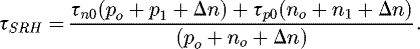 (1)
(1)
The SRH densities n1 and p1 represent the electrons and holes concentration when the defect and Fermi level coincide, and are expressed as: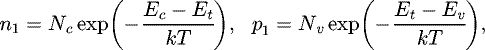 (2)
(2)
where n0 and p0 represent the carrier densities in the conduction and valence band respectively at thermal equilibrium. Nc and Nv are the effective densities of states in the conduction and valence band respectively. The capture time constants for electrons and holes, τn0 and τp0 respectively, are given by: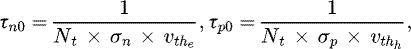 (3)with
  and
and  the electron and hole thermal velocity respectively.
Introducing the symmetry factor k, defined as,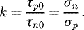 (4)
(4)
Equation (1) can be rewritten in terms of the symmetry factor: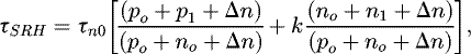 (5)
(5)
Et, Nt and σ are characteristic to the impurity's nature and allow its identification. TDLS consists in fitting equation (1) to experimental temperature-dependent lifetime data in order to extract these quantities. It is therefore necessary to consider the temperature dependence of all the parameters in equation (1).
2.2 Parameters temperature dependence
The temperature dependence of the capture time constants τn0τp0 arises from the electron and hole thermal velocity  and the capture cross sections σn and σp.
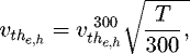 (6)where vthe,h300 the thermal velocities at room temperature, calculated as:
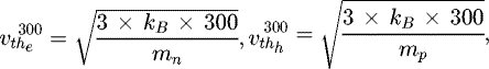 (7)with mn = 0.26mo and mp = 0.39mo the electron and hole masses at 300 K and m0 the electron mass at rest.
The temperature dependence of the capture cross sections depends on the capture process involved. In silicon, Excitonic Auger [19] (EA) and multi-phonon emission [20] (MPE) processes are dominant [21]. The EA process is relevant to deep impurities. When a free exciton meets an impurity, one of the particles is captured and the excess energy is transferred to the second one. Two subsequent EA processes are necessary for a complete electron-hole recombination. In this case, the capture cross section shows a negative power-law temperature dependence and is expressed as [22]: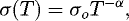 (8)with α > 0.
In the MPE mechanism model, lattice vibrations cause for the free and bound carrier levels to cross which results in the capture of a free carrier. The excessive energy is dissipated through the emission of multiple phonons. MPE capture mechanism has a thermally activated behaviour, the capture cross section is expressed as: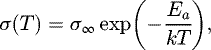 (9)
(9)
Ea being the energy that a free electron from the BC has to overcome in order to be captured by the defect.
For the effective densities of states, Nc and Nv, we consider the temperature dependence of the effective masses. They are expressed as [23]: (10)where k and h are Boltzmann and Planck's constants respectively,
  and
and  the density-of-states effective masses in the BC and BV respectively given by [24]:
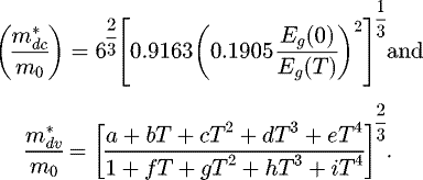 (11)
(11)
With a, b, c, d, e, f, g, h and i constants given in Table 1 [24].
In equation (11), Eg (0) is the energy gap of silicon at 0K and is equal to 1.17 eV, the temperature dependence of the energy band gap is expressed as [25]: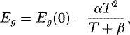 (12)where α = 73 × 10−4 ev/K is a temperature coefficient and β = 636 K a temperature offset.
The range in which TDLS data are acquired requires to also consider the temperature dependence of the carrier density. We distinguish three regimes:
-
the freeze-out regime at low temperatures where the thermal energy is not sufficient to ionize the dopants atoms (po (T) < NA).
-
the extrinsic regime at intermediate temperatures where the carrier density equals the doping (po (T) = NA).
-
the intrinsic regime at high temperatures where the semiconductor is dominated by intrinsic conduction (po (T) > NA).
Considering p-type silicon, the majority carrier density at thermal equilibrium is a piecewise-defined function, expressed as [26]: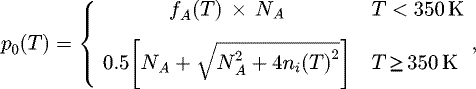 (13)where fA is the ionization level, the fraction of ionized acceptor atoms:
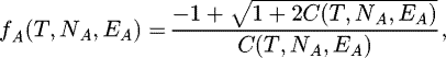 (14)
with
(14)
with 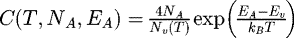 .
.
The minority carrier density is calculated using: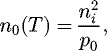 (15)with ni the intrinsic carrier density, function of the effective density of states in the BC and BV and the bandgap energy Eg:
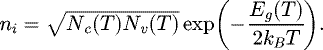 (16)
(16)
3 Results
3.1 Gold contamination
In the silicon lattice, gold occupies substitutional sites and acts as a two-level defect [27] thus introducing two energy levels, a donor and an acceptor [28,29].
The temperature dependence of the capture cross sections associated to the gold levels was measured in n-type Si [30]. As gold is not known for forming complexes in Si, the capture cross sections are expected to be the same in p-type Si. The activation energy and capture cross sections for the gold levels are summarized in Table 2.
In p-type Si, the lifetime of minority carriers is dominated by the donor level [31–33].
We consider gold-contaminated p-type silicon with a Boron doping of NA = 1015 cm−3 and a gold concentration of Nt = 1012 cm−3. At low and intermediate temperatures (T < 500 K), for a low injection level (Δn ≪ p0 + n0) and p-type doping (n0 ≪ p0), equation (1) reduces to: (17)
(17)
At high temperature, the approximation does not hold, n0 increases as we enter the intrinsic conduction. At low temperature, as p1 → 0 the lifetime can be approximated by τn0 (Eq. (3)) as shown in Figure 1. The thermal velocity being known, Nt × σn can be determined. In the hypothesis of a known impurity concentration Nt, fitting the low temperature part of the SRH lifetime to equation (3) and multiplying the result by the electron thermal velocity vthe, an electron capture cross section of σn = 2.12 × 10⁻¹¹T −1.96 is obtained.
To extract the energy depth ΔEt, we use the Defect Parameter Solution Surface (DPSS) method developed by Rein and Glunz [15]. The method consists of least-squares-fitting the TDLS data while varying the energy depth ΔEt through the whole band gap (ΔEt ∈ [0, 1.12 eV]) and optimizing the symmetry factor k for each energy depth. The DPSS results in two curves, the optimal symmetry factor k-DPSS and the least square fitting error Chi2-DPSS as a function of Ec − Et.
Applying the DPSS analysis to the TDLS curve of Figure 1, it results in the two curves of Figure 2. We get two solutions as the least squares fit error is minimized by two distinct defect parameters, one in each half of the band gap with the same energy depth located at Ec − Et = 0.34 eV and Et − Ev = 0.34 eV with optimal k values of k = 1.16 and k = 0 respectively.
Activation energy and capture cross sections of gold donor, gold acceptor and substitutional nickel in silicon.
 |
Fig. 1 Calculated TDLS curve (thick solid line) of Au-contaminated p-type Si ([Au] = 1012cm−3, NA = 1015cm−3) and the electron capture time constant τn0 (dashed line). Below 250 K, approximating the TDLS curve by τn0 allows the T-dependent capture cross-section σn (T) extraction. |
 |
Fig. 2 Resulting DPSS diagram obtained from least-squares-fitting the TDLS lifetime data shown in Figure 1 using the extracted capture cross section σn (T) = 2.12 × 10⁻¹¹ × T −1.96. Two solutions are obtained from Chi2-DPSS curve minimum position, Ec − Et = 0.34 eV with k = 1.16 and Et − Ev = 0.34 eV with k = 0. With a smaller Chi2 value by almost two orders of magnitude, the solution in the second half of the bandgap is identified as the true solution. |
3.2 Nickel contamination
At room temperature, only substitutional nickel remains in Si as unstable interstitial nickel disappears by outdiffusion or precipitation [7]. The parameters associated to substitutional Nickel (Nis) were determined by Rein [26] using TDLS (Tab. 2) and were used for the modeling of the lifetime curves.
We consider nickel-contaminated p-type silicon with a Boron doping of NA = 1015 cm−3 and a nickel concentration of Nt = 1012cm−3. At low and intermediate temperatures (T < 500 K), for a low injection level (Δn ≪ p0 + n0), p-type doping (n0 ≪ p0) and for a defect in the upper half of the gap, equation (1) reduces to: (18)
(18)
At low temperature, the lifetime is approximated by the electron capture time constant τn0 (Eq. (3)) as shown in Figure 3. In the hypothesis of a known impurity concentration Nt, fitting the low temperature part of the SRH lifetime to equation (3) leads to an electron capture cross section of σn = 4.56 × 10⁻¹¹T −2.4.
Applying the DPSS analysis to the TDLS curve of Figure 3 using this extracted capture cross section results in the two curves of Figure 4.
Two solutions are highlighted by the DPSS-Chi2 curve minimums, one in each half of the band gap located at Ec − Et = 0.40 eV and Et − Ev = 0.41 eV with optimal DPSS-k values of k = 0.83 and k = 0.16 respectively. The solution in the second half of the gap (Et − Ev = 0.41 eV) representing the global minimum of the DPSS-Chi2 curve could stand out as the true solution, however the solution does not correspond to the true level of Nickel.
Applying the DPSS using the τn0 value used for the TDLS curve modeling gives a distinct solution at the right position of the Ni defect level Ec − Et = 0.40 eV (DPSS diagram not shown). This means that the small offset that appears in Figure 3 resulting from the approximation of the low temperature part of the TDLS curve by equation (3) is enough to throw the solution in the wrong half of the gap.
Since we can accurately extract the temperature dependence of τn0 from the Ni-TDLS curve at low temperature, we can modify the DPSS optimized parameters to reduce the error related to the approximation. Inputting only the temperature dependence of τn0 in the least-squares-fitting routine, we carry a DPSS analysis optimizing both the symmetry factor k, and the Nt × σ0 product. The DPSS diagram now results in three curves, the optimal symmetry factor k-DPSS, the Nt × σ0 product denoted A-DPSS and the least square fitting error Chi2 as a function of Ec − Et.
Using the extracted temperature dependence of τn0 ∝ T 2.4, it results in the three curves of Figure 5. Two solutions are highlighted by the Chi2-DPSS curve minimum, one in each half of the band gap with the same energy depth and close values of A = Nt × σ0. The solutions are located at Ec − Et = 0.40 eV and Et − Ev = 0.41 eV with optimal k-DPSS and A-DPSS values of k = 0.89, A = 49.5 cm−1 and k = 0.28, A = 46.7 cm−1 respectively.
 |
Fig. 3 Calculated TDLS curve (thick solid line) of Ni-contaminated p-type ([Ni] = 1012cm−3, NA = 1015cm−3) and the electron capture time constant τn0 (dashed line). Below 270K, approximating the TDLS curve by τn0 allows the T-dependent capture cross-section σn (T) extraction. |
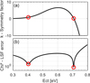 |
Fig. 4 Resulting DPSS diagram obtained from least-squares-fitting the TDLS lifetime data shown in Figure 1 using the extracted capture cross section σn (T) = 4.56 × 10⁻¹¹ × T −2.4. Two solutions are obtained from Chi2-DPSS curve minimum position, Ec − Et = 0.40 eV with k = 0.83 and Et − Ev = 0.41 eV with k = 0.16. Even though the second solution shows a lower Chi2 value, the solution does not correspond to the true Ni defect level. |
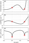 |
Fig. 5 Resulting DPSS diagram obtained from least-squares-fitting the TDLS lifetime data shown in Figure 1 only using the extracted temperature dependence of the capture cross section (T −2.4) as an input. The diagram results in three curves, (a) the optimized symmetry factor k (b) optimized Nt × σ0 denoted A-DPSS and (c) the least-squares fit error Chi2. Two solutions are highlighted by the Chi2-DPSS curve minimum position, Ec − Et = 0.40 eV with k = 0.89, A = 49.5 cm−1 and Et − Ev = 0.41 eV with k = 0.28, A = 46.7 cm−1. The Chi2-DPSS curve allows the true defect parameters identification from the position of its global minimum in the upper bandgap half. |
4 Discussion
The analysis of temperature-dependent lifetime data does not allow to quantify unknown impurities as the impurity concentration Nt cannot be separated from the product Nt × σn (T).
We can however extract the temperature dependence of the electron capture cross section in the case of gold or nickel contamination in p-type Si. At low temperature, the temperature dependence of the lifetime arises from the electron capture cross section σn (T) and the known electron thermal velocity  .
.
The DPSS analysis of the Au-contaminated p-type Si TDLS curve highlighted two solutions located at Ec − Et = 0.34 eV and Et − Ev = 0.34 eV with optimal k values of k = 1.16 and k = 0 respectively. These two solutions differ in their DPSS-Chi2 value. In this case, the method allows us to determine which of the solutions correspond to the true defect parameter as the Chi² value of the solution Et − Ev = 0.34 eV and k = 0 in the lower half of the gap is almost two orders of magnitude smaller than the solution in the upper half of the gap. The corresponding optimized k-DPSS value of k = 0 is due to the fact that the TDLS curve does not depend on the symmetry factor as given by the approximation of equation (18). Therefore, in the case of gold we cannot deduce a value for the hole capture cross section from the k-DPSS result.
For the DPSS results extracted from the TDLS curve of Ni-contaminated p-type Si, although the solution in the lower half of the bandgap Et − Ev = 0.41 eV is distinguished by a lower Chi2 value in Figure 4, it does not correspond to the true Ni level. Both solutions being of the same order of magnitude, we cannot formally conclude regarding the position of the defect level. The ambiguity in these results arises from the approximation of the lifetime data at low temperature. For DPSS to yield unambiguous results, an accurate determination of the electron capture time constant  is necessary.
In the case of both Ni and Au, as we can accurately extract the temperature dependence of τn0 at low temperature, instead of inputting τn0 in the DPSS least-squares-fitting routine, we now only input its temperature dependence and optimize both the symmetry factor k-DPSS and the Nt × σ0 product denoted A-DPSS. In the case of Nickel, the solutions are located at Ec − Et = 0.40 eV and Et − Ev = 0.41eV with optimal k-DPSS and A-DPSS values of k = 0.89, A = 49.5 cm−1 and k = 0.28, A = 46.7 cm−1 respectively. The solution in the upper bandgap half (Ec − Et = 0.40 eV) has a Chi2-DPSS value more than an order of magnitude smaller than the solution in the lower bandgap half. Therefore, Ec − Et = 0.40 eV, k = 0.89 and A = 49.5 cm−1 represent the true defect parameters. In the hypothesis of a known impurity concentration (here Nt = 1012cm−3), using the A-DPSS value and the extracted temperature dependence, the total electron capture cross section is given by σn = 4.95 × 10⁻¹¹T −2.4.
The k-DPSS value results in an almost 30% overestimation of the symmetry factor k = 0.7 used for the TDLS curve modeling leading to an underestimation of the hole capture cross section σp, but the result remains in the same order of magnitude. Since the capture cross section of both holes and electrons follows the same temperature law, using the k-DPSS value we can deduce the hole capture cross section at 300 K σp: .
.
The capture cross section values used for the temperature-dependent lifetime modeling for Nickel were given by Rein [26]. The given value of the hole capture cross section was extracted using the optimized k-DPSS value assuming that the capture process for both holes and electrons is the same, the symmetry factor being temperature independent. Thus, the hole capture cross section was assigned the same temperature dependence as the one extracted for electrons. However, the hypothesis of a constant symmetry factor does not hold for all impurities according to the literature as given by the capture cross sections of Au [30], Fe [34] and Ti [35]. The hole capture cross section has the effect of modifying both quantitatively and qualitatively the TDLS curve for Ni-contaminated Si depending on its model.
All the temperature-dependent lifetime data were calculated in the 120-650K range. Extracting the temperature dependence of the capture cross section σn requires for the data to be obtained at sufficiently low temperatures. Not including the high temperature part of the curve in the fit routine does not prevent the energy depth and position of the defect to be determined.
Measured TDLS data are subject to uncertainties. The DPSS-Chi2 curve allows to estimate an error on the extracted defect parameters from the minimum peak width by setting a limit for the tolerated DPSS-Chi2 value.
This study is a preliminary study for the development of a characterization bench based on the microwave phase-shift technique (μW-PS) for the determination of impurities in silicon. μW-PS [36] is a sensitive (109cm−3 limit [37]), contactless technique carried out at low level of carrier injection based on the measurement of the phase-shift between the modulated light excitation signal and the intensity of the reflected microwaves.
5 Conclusion
Recombination through defect levels in the band gap of silicon has the impact of limiting the minority carrier lifetime inducing efficiency losses in crystalline silicon. The study of the temperature-dependent lifetime of minority carriers in gold and nickel-contaminated p-type Si showed that the exploitation of the TDLS curves allow to identify both impurities through their defect level ΔEt and electron capture cross section σn (T). TDLS does not allow to quantify the impurities through the determination of Nt and data have to be acquired over a wide range from low to high temperatures. The low temperature part allows the temperature-dependence of the electron capture time constant τn0 to be extracted while the whole curve is used for the defect parameter solution surface (DPSS) fit routine. Optimizing both the symmetry factor k and the Nt × σ0 product, the DPSS allows the unambiguous determination of the defect energy depth and bandgap half position.
The development of an experimental setup for TDLS data acquisition based on the microwave phase-shift technique is currently ongoing and will allow to compare simulation results with experimental data. A secondary goal will be to extend the study to other detrimental impurities such as iron and chromium.
Author contribution statement
S. Dehili conducted the modeling study and wrote the manuscript. D. Barakel, L. Ottaviani and O. Palais supervised the work and the data analysis. All authors commented on previous versions of the manuscript, read and approved the final manuscript.
References
- International Energy agency − IEA, Renewable Power, Paris, 2020 [Google Scholar]
- Fraunhofer Institute for Solar Energy Systems ISE, Photovoltaics Report, Freiburg, 2020 [Google Scholar]
- J.R. Davis, A. Rohatgi, R.H. Hopkins, P.D. Blais, P. Rai-Choudhury, J.R. McCormick, H.C. Mollenkopf, IEEE Trans. Electron Devices 27, 677 (1980) [Google Scholar]
- J. Schmidt, B. Lim, D. Walter, K. Bothe, S. Gatz, T. Dullweber, P.P. Altermatt, IEEE J. Photovoltaics 3, 114 (2013) [Google Scholar]
- H. Savin, M. Yli-Koski, A. Haarahiltunen, Appl. Phys. Lett. 95, 15 (2009) [Google Scholar]
- A. Inglese, A. Focareta, F. Schindler, J. Schön, J. Lindroos, M.C. Schubert, H. Savin, Energy Procedia 92, 808 (2016) [Google Scholar]
- K. Graff, Metal Impurities in Silicon-Device Fabrication (Springer Science, Berlin, 2013) [Google Scholar]
- A.A. Istratov, E.R. Weber, Appl. Phys. A 66, 123 (1998) [Google Scholar]
- J. Lindroos, D.P. Fenning, D.J. Backlund, E. Verlage, A. Gorgulla, S.K. Estreicher, H. Savin, T. Buonassisi, J. Appl. Phys. 113, 204906 (2013) [Google Scholar]
- E.R. Weber, Appl. Phys. A Solids Surfaces 30, 1 (1983) [Google Scholar]
- T. Hosoya, Y. Ozaki, K. Hirata, J. Electrochem. Soc. 132, 2436 (1985) [Google Scholar]
- A. Inglese, J. Lindroos, H. Vahlman, H. Savin, J. Appl. Phys. 120, (2016) [Google Scholar]
- B.B. Paudyal, K.R. McIntosh, D.H. MacDonald, G. Coletti, J. Appl. Phys. 107, 2 (2010) [Google Scholar]
- A.E. Morishige, M.A. Jensen, D.B. Needleman, K. Nakayashiki, J. Hofstetter, T.T.A. Li, T. Buonassisi, 2017 IEEE 44th Photovolt. Spec. Conf. PVSC 2017, 1 (2017) [Google Scholar]
- S. Rein, S.W. Glunz, Appl. Phys. Lett. 82, 1054 (2003) [Google Scholar]
- C. Sun, F.E. Rougieux, D. Macdonald, J. Appl. Phys. 115, (2014) [Google Scholar]
- W. Shockley, W.T. Read, Phys. Rev. 87, 835 (1952) [CrossRef] [Google Scholar]
- R.N. Hall, Phys. Rev. 87, 387 (1952) [Google Scholar]
- A. Hangleiter, Phys. Rev. B 37, 2594 (1988) [Google Scholar]
- D.V. Lang, C.H. Henry, Phys. Rev. B 15, 989 (1977) [Google Scholar]
- F.E. Rougieux, C. Sun, D. Macdonald, Sol. Energy Mater. Sol. Cells 187, 263 (2018) [Google Scholar]
- A. Hangleiter, Phys. Rev. B 35, 9149 (1987) [Google Scholar]
- M.A. Green, J. Appl. Phys. 67, 2944 (1990) [CrossRef] [Google Scholar]
- J.E. Lang, F.L. Madarasz, P.M. Hemenger, J. Appl. Phys. 54, 3612 (1983) [CrossRef] [Google Scholar]
- S.M. Sze, K.K. Ng, Physics of Semiconductor Devices , 3rd edn. (Wiley, NJ, 2007) [Google Scholar]
- S. Rein, Lifetime Spectroscopy (Springer-Verlag, Berlin/Heidelberg, 2005) [Google Scholar]
- J. Utzig, W. Schröter, Appl. Phys. Lett. 45, 761 (1984) [Google Scholar]
- E.A. Taft, F.H. Horn, Phys. Rev. 93, 64 (1954) [Google Scholar]
- C.B. Collins, R.O. Carlson, C.J. Gallagher, Phys. Rev. 105, 1168 (1957) [Google Scholar]
- R.H. Wu, A.R. Peaker, Solid-State Electron. 25, 643 (1982) [Google Scholar]
- G. Bemski, Phys. Rev. 111, 1515 (1958) [Google Scholar]
- C.C. Abbas, IEEE Trans. Electron Devices 31, 1428 (1984) [Google Scholar]
- K. Watanabe, C. Munakata, Semicond. Sci. Technol. 8, 230 (1993) [Google Scholar]
- B.B. Paudyal, K.R. McIntosh, D.H. MacDonald, in 34th IEEE Photovolt. Spec. Conf. (IEE, Philadelphia, 2009), p. 001588 [Google Scholar]
- A.C. Wang, C.T. Sah, J. Appl. Phys. 56, 1021 (1984) [Google Scholar]
- O. Palais, J. Gervais, E. Yakimov, S. Martinuzzi, Opt. Mater. (Amst). 162, 157 (2000) [Google Scholar]
- O. Palais, Solid State Phenom. 79, 267 (2001) [Google Scholar]
Cite this article as: Sarra Dehili, Damien Barakel, Laurent Ottaviani, Olivier Palais, Nickel and gold identification in p-type silicon through TDLS: a modeling study, Eur. Phys. J. Appl. Phys. 94, 10101 (2021)
All Tables
Activation energy and capture cross sections of gold donor, gold acceptor and substitutional nickel in silicon.
All Figures
|
Fig. 1 Calculated TDLS curve (thick solid line) of Au-contaminated p-type Si ([Au] = 1012cm−3, NA = 1015cm−3) and the electron capture time constant τn0 (dashed line). Below 250 K, approximating the TDLS curve by τn0 allows the T-dependent capture cross-section σn (T) extraction. |
| In the text | |
|
Fig. 2 Resulting DPSS diagram obtained from least-squares-fitting the TDLS lifetime data shown in Figure 1 using the extracted capture cross section σn (T) = 2.12 × 10⁻¹¹ × T −1.96. Two solutions are obtained from Chi2-DPSS curve minimum position, Ec − Et = 0.34 eV with k = 1.16 and Et − Ev = 0.34 eV with k = 0. With a smaller Chi2 value by almost two orders of magnitude, the solution in the second half of the bandgap is identified as the true solution. |
| In the text | |
|
Fig. 3 Calculated TDLS curve (thick solid line) of Ni-contaminated p-type ([Ni] = 1012cm−3, NA = 1015cm−3) and the electron capture time constant τn0 (dashed line). Below 270K, approximating the TDLS curve by τn0 allows the T-dependent capture cross-section σn (T) extraction. |
| In the text | |
|
Fig. 4 Resulting DPSS diagram obtained from least-squares-fitting the TDLS lifetime data shown in Figure 1 using the extracted capture cross section σn (T) = 4.56 × 10⁻¹¹ × T −2.4. Two solutions are obtained from Chi2-DPSS curve minimum position, Ec − Et = 0.40 eV with k = 0.83 and Et − Ev = 0.41 eV with k = 0.16. Even though the second solution shows a lower Chi2 value, the solution does not correspond to the true Ni defect level. |
| In the text | |
|
Fig. 5 Resulting DPSS diagram obtained from least-squares-fitting the TDLS lifetime data shown in Figure 1 only using the extracted temperature dependence of the capture cross section (T −2.4) as an input. The diagram results in three curves, (a) the optimized symmetry factor k (b) optimized Nt × σ0 denoted A-DPSS and (c) the least-squares fit error Chi2. Two solutions are highlighted by the Chi2-DPSS curve minimum position, Ec − Et = 0.40 eV with k = 0.89, A = 49.5 cm−1 and Et − Ev = 0.41 eV with k = 0.28, A = 46.7 cm−1. The Chi2-DPSS curve allows the true defect parameters identification from the position of its global minimum in the upper bandgap half. |
| In the text | |
Current usage metrics show cumulative count of Article Views (full-text article views including HTML views, PDF and ePub downloads, according to the available data) and Abstracts Views on Vision4Press platform.
Data correspond to usage on the plateform after 2015. The current usage metrics is available 48-96 hours after online publication and is updated daily on week days.
Initial download of the metrics may take a while.