| Issue |
Eur. Phys. J. Appl. Phys.
Volume 99, 2024
|
|
|---|---|---|
| Article Number | 4 | |
| Number of page(s) | 9 | |
| DOI | https://doi.org/10.1051/epjap/2023230208 | |
| Published online | 07 March 2024 | |
https://doi.org/10.1051/epjap/2023230208
Original Article
Diffusion models of grown-in and implanted p-type dopant in III-V semiconductor compounds
Université de Rouen Normandie, Laboratoire CRISMAT UMR 6508, CNRS, ENSICAEN, Université de Caen, 6 boulevard du Maréchal Juin, 14050, Caen, France
* e-mail: This email address is being protected from spambots. You need JavaScript enabled to view it.
Received:
30
October
2023
Accepted:
18
December
2023
Published online: 7 March 2024
Abstract
This research shows that the diffusion of grown-in and implanted Be atoms in III-V considered semiconductor materials, such as the Liquid-Encapsulated Czochralski-grown (LEC) GaAs as well as the Gas-Source Molecular Beam Epitaxy (GSMBE) In0.53Ga0.47As, In0.73Ga0.27As0.58P0.42, In0.53Ga0.47As/In0.73Ga0.27As0.58P0.42, In0.53Ga0.47As/InP compounds, taking place during the Rapid Thermal Annealing (RTA) process, is perfectly well explained by the “full” version of the kick-out mechanism operating through singly positively ionized Be interstitials and group III self-interstitial ions (Ga, In) in all their states of positive charge including neutral. Numerical solutions of the differential equations, corresponding to the considered system of diffusion reactions, have been calculated using the finite difference approach and our elaborate finite difference-Bairstow method. Such a model naturally emerges from most research works, including ours, in the considered field, over the last decades and makes it possible to “reconcile” their different diffusion models. In this study, we also present and analyze the Secondary Ion Mass Spectrometry (SIMS) profiles of the distribution of implanted Be in GaAs at an energy of 100 keV with a high dose of 1.0 ⋅ 1015cm−2 and annealed at temperatures ranging from 700 to 850 °C for à time ranging from 60 to 240s.
Key words: Diffusion / semiconductors / GSMBE / SIMS / RTA
© S.D. Koumetz, Published by EDP Sciences, 2024
 This article is distributed under the terms of the Creative Commons Attribution License https://creativecommons.org/licenses/by/4.0 which permits unrestricted use, distribution, and reproduction in any medium, provided the original author(s) and source are credited.
1 Introduction
With regard to the diffusion of p-type dopants in III-V compounds, since the 1980 s some researchers have continued to use the dissociative mechanism, while others have preferred to carry out their work using the newly discovered diffusion mechanism known as ‘‘kick-out’’, in accordance with forced (kicked) exchanges between the p-type dopant interstitial acceptors, having two valence electrons, and the covalent atoms III of the semiconductor compounds III-V, having three valence electrons.
Since its proposal [1], the kick-out mechanism of Zn diffusion in GaAs, in accordance with most authors, had been used to explain the diffusion of Be in GaAs and related compounds [2–10].
Most research works show that Be interstitials are singly positively charged. Indeed, according to the experimental and theoretical studies of Be diffusion in GaAs and related compounds, the values of 0 [9], 1+ [2–8,10] and 2+ [11] have been proposed for Be interstitial charge state.
Regarding the charge state of the group III self-interstitials participating in the kick-out mechanism, the publications of the last decades very clearly show that they can have all the positives charges including neutral. Models including a single type of self-interstitials or their different combinations, have been proposed.
So, theoretical and experimental research had shown that the dominant charge state of Ga self-interstitials in p-type GaAs compounds can be 1+ [4–6,8,12], 2+ [2,3,7,13], 1+ or 2+ and 3+ [14], 2+ or 3+ [15], 1+ or 3+ [16], 2+ and 3+ [17], 0 and 1+ [18,19], 1+, 2+ and 3+ [20,21].
As for indium self-interstitials in p-type InP, the theoretical works have predicted the following charge states: 1+ [22] as well as 1+ or 2+ and 3+ [23].
In our previous work relative to grown-in Be diffusion in the ternary and quaternary III-V compounds, we have proposed a simple kick-out mechanism, involving neutral Be interstitials and singly positively charges Ga, In self-interstitials, associated however with an extended defect formation assumption [24].
More recently, we have demonstrated that a grown-in Be diffusion in InGaAs and InGaAsP compounds, taking place always during the first minutes of the RTA process, can be well described by a combined kick-out and dissociative mechanism [25], implying neutral Be interstitials, singly positively charged Ga, In self-interstitials and singly positively charged Ga, In vacancies [26].
In the same publication [26], we mentioned that the obtained experimental results were also successfully explained by the model of the kick-out mechanism using neutral Be interstitials and all the types of positively charged, including neutral, Ga and In self-interstitials.
This our latest research shows well that finally a grown-in Be diffusion in the ternary InGaAs and quaternary InGaAsP compounds as well as in the ternary/quaternary InGaAs/InGaAsP and ternary/binary InGaAs/InP heterostructures is still perfectly described by the ‘‘full’’ version of the kick-out mechanism involving singly positively charged Be interstitials, however, and neutral, singly, doubly, triply positively charged Ga, In self-interstitials. So, the full kick-out model permits also describe a grown-in Be diffusion in the binary InP compounds.
According to this study, the proposed “full” kick-out mechanism explains also very well an implanted Be diffusion in the ternary InGaAs compounds. Its partial version, using only doubly positively charged Ga self-interstitial species with the application of the plus-one approach [27], was very successfully applied in the case of implanted Be diffusion in GaAs for RTA temperatures ranging from 700 to 800 °C in our previous work [28,29]. The results of the present work show that at annealing temperature of 850 °C the action of the singly and triply charged Ga self −interstitials, notably, becomes important and adds to that of the doubly charged Ga species.
It should be noted that another version of the “full” kick-out mechanism with neutral Be interstitial species, only mentioned in our previous article [26], did not allow however to explain very well an implanted Be diffusion in the ternary InGaAs compounds.
2 Results and analysis
The detailed descriptions of the experimental procedures concerning a grown-in Be diffusion in InGaAs, InGaAsP, InGaAs/InGaAsP, InGaAs/InP compounds and an implanted Be diffusion in GaAs compounds are given in references [24,26] and [28,29], respectively.
2.1 Grown-in Be diffusion
In the present research work, concerning a grown-in Be diffusion in the binary, ternary and quaternary III-V Gas-Source Molecular Beam Epitaxy (GSMBE) compounds, and through their heterojunctions, taking place during the Rapid Thermal Annealing (RTA) process, the proposed full kick-out mechanism where exchanges between singly positively charged Be interstitials ( ) and active singly negatively charged Be substitutionals (
 ), occupied Ga, In (group III) sites, are realized via Ga, In self-interstitials in all their positive charge states, including neutral, according to the following 4 diffusion reactions:
 (1)
(1)
where i = 0,1,2,3;  indicate, respectively, neutral, singly, doubly, triply positively charged Ga, In self-interstitials; h+ is a free hole; kf and kr denote forward and reverse rate constants, respectively, associated with reactions (1).
With regard to the secondary effect that Ga, In vacancies in all their states of negative charge, including neutral, can exert on the neutral and charged Ga, In self-interstitials via their generation-recombination process, we concluded, in accordance with our simulation results, that the concentrations of Ga, In vacancies in all their charge state and at all annealing temperatures in all studied materials are such that they do not exert a significant action that could lead to appreciable modification of the simulation results. In this way, the secondary effect of Ga, In vacancies exerted on Ga, In self-interstitials, being negligible, has not been taken into account as was the case, for example, in the modeling of grown-in Be diffusion in GaAs, presented by Hu et al. [4].
Numerical solutions of the partial differential equations, corresponding to the reactions (1), have been calculated using the finite difference approach [25] and our elaborate finite difference-Bairstow method [26,28,29], which of course produced the identical results of the simulations. The advantage of the latter technique over the former is that it's simpler and much faster to use during simulation processes [26,28,29]. For diffusion through heterojunctions, the boundary conditions at the interfaces have been applied [24].
The temperature dependent intrinsic electron concentration values for InGaAs, InGaAsP, InP compounds were deduced from its band gap Eg(T) and electron, hole effective masses  , respectively, according to the following expression [30]:
 (2)
(2)
where h, kB and T are the Planck constant, the Boltzmann constant and the absolute temperature, respectively.
In this way, the intrinsic electron concentrations, as function of temperature in the Arrhenius equation form, have been obtained for the considered materials:
 (3a)
(3a)
 (3b)
(3b)
 (3c)
(3c)
The other diffusion parameters values, used in the simulations, were optimized to give a best fit to our experimental profiles.
The obtained data for the 3 studied compounds have allowed us to determine the Arrhenius equations for the used diffusion parameters of which the pre-exponential factors and the activation energies are presented in Tables 1–3 where  and
and  represent concentrations and diffusion coefficients of
  species, respectively.
Concerning the charge balance of the diffusing species, the suggested local charge neutrality condition, in view of an insignificant secondary effect exercised by Ga, In vacancies on Ga, In self-interstitials, as well as the semiconductor mass action low, lead to the following local hole concentration:
 (4)
(4)
By way of example of the results of our simulations, based on the full kick-out mechanism, Figures 1–4 show the Be Secondary Ion Mass Spectrometry (SIMS) data before and after RTA at a temperature of 800 °C as well as the simulation profiles obtained for the Be diffusion in InGaAs, InGaAsP, InGaAs/InGaAsP and InGaAs/InP compounds for the annealing times of 60, 120, 30 and 180 s, respectively.
The Arrhenius equation components for the diffusion parameter values in InGaAs samples.
The Arrhenius equation components for the diffusion parameter values in InGaAsP samples.
The Arrhenius equation components for the diffusion parameter values in InP samples.
 |
Fig. 1 SIMS profiles of grown-in Be before and after annealing of InGaAs sample at 800 °C for 60 s and the simulated profile. |
 |
Fig. 2 SIMS profiles of grown-in Be before and after annealing of InGaAsP sample at 800 °C for 120 s and the simulated profile. |
 |
Fig. 3 SIMS profiles of grown-in Be before and after annealing of InGaAs/InGaAsP sample at 800 °C for 30 s and the simulated profile. |
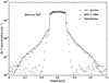 |
Fig. 4 SIMS profiles of grown-in Be before and after annealing of InGaAs/InP sample at 800 °C for 180 s and the simulated profile. |
2.2 Implanted Be diffusion
During our study of an implanted Be in InGaAs, we found that the best fitting results give the proposed full model of the kick-out mechanism. In this study we used the experimental results obtained by Rao, Moore, Dietrich in their work concerning the implants in InGaAs (see Fig. 5) [31] and those presented by Maier, Selders in their study relating to the RTA of beryllium-implanted InGaAs (see Fig. 6) [32].
Figure 5 shows SIMS profiles of implanted Be in In 0.53Ga0.47As at an energy of 40 keV with a dose of 5.0 ⋅ 1013cm−2 before and after rapid thermal annealing at 850 °C for 5 s [31].
Figure 6 shows SIMS unannealed and rapid thermal annealed profiles of Be implanted in In 0.53Ga0.47As at an energy of 200 eV with a dose of 6.0 ⋅ 1014cm−2 where RTA was performed at a temperature of 800 °C for 1 s [32].
We can see that the simulated profiles obtained by the application of the proposed full kick-out model, shown by Figures 5 and 6, fit very satisfactory the corresponding experimental profiles. As in the case of the diffusion of Be implanted in GaAs [28,29], the plus-one approach [27] was used in these modelings.
To explain the obtained experimental results, concerning the transient enhanced diffusion of an implanted Be in GaAs during the first minutes of the RTA process, we have proposed in the previous work the kick-out mechanism, in its “simplest” version, based on singly positively charged Be interstitials and doubly positively charged Ga self-interstitials [28,29]. This version of the kick-out mechanism has been widely used in the past to explain notably Zn diffusion in GaAs [2,3,7]. In fact, it was the only mechanism among a multitude of others studied capable to explain very well the obtained experimental results [28,29].
However, even if for annealing temperatures of 700, 750 and 800 °C of Be implanted in GaAs with the dose of 1.0 ⋅ 1014cm−2, the proposed “full” model of kick-out mechanism did not really improve the simulation results, already excellent, obtained with the “simple” kick-out model in our previous work [28,29], we realized that the simulation results given by the full model in the case of RTA annealing at 850 °C are much better than those based on the simple model. Indeed, at this annealing temperature the action of singly and triply charged Ga auto-interstitials, notably, becomes significant and is added to that of the doubly charged Ga ions.
Figures 7–10 show SIMS distribution profiles of Be implanted at an energy of 100 keV in GaAs with a dose of 1.0 ⋅ 1014cm−2 unannealed and annealed at 700, 750, 800 and 850 °C for 60, 120, 180 and 240 s at each temperature. The experimental conditions of these implants have already been presented in our previous work [28,29], but their experimental data have never yet been published.
Unlike the Be implants at an energy 100 keV in GaAs with doses of 1.0 ⋅ 1013 and 1.0 ⋅ 1014cm−2 which did not show any out-diffusion of Be during rapid thermal annealing at the temperatures and durations studied [28,29], and therefore kept their doses, the Be implants at the same energy with a dose of 1.0 ⋅ 1015cm−2 very clearly show the Be out-diffusion increasing with annealing temperature and time (Figs. 7–10).
The Be profiles at 700 °C for all considered annealing times being almost identical, their average remaining dose in GaAs is 6.9 ⋅ 1014cm−2 (Fig. 7). For the higher temperatures studied, the remaining Be dose varies as follows: at 750 °C from 7.0 ⋅ 1014cm−2 for 60 s to 5.9 ⋅ 1014cm−2 for 240 s (Fig. 8), at 800 °C from 5.7 ⋅ 1014cm−2 for 60 s to 4.1 ⋅ 1014cm−2 for 240 s (Fig. 9) and at 850 °C from 4.5 ⋅ 1014cm−2 for 60 s to 3.4 ⋅ 1014cm−2 for 240 s (Fig. 10).
 |
Fig. 5 SIMS profiles of implanted Be in InGaAs at an energy of 40 eV with a dose of 5.0 ⋅ 1013cm−2 before and after annealing at 850 °C for 5 s (obtained by Rao et al. [31]), and the simulated profile. |
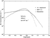 |
Fig. 6 SIMS profiles of implanted Be in InGaAs at an energy of 200 keV with a dose of 6.0 ⋅ 1014cm−2 before and after annealing at 800 °C for 1 s (obtained by Maier et al. [32]), and the simulated profile. |
 |
Fig. 7 The SIMS profiles of implanted Be in GaAs at an energy of 100 keV with a dose of 1.0 ⋅ 1015cm−2 before and after annealing at 700 °C for 60, 120, 180, 240 s. |
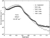 |
Fig. 8 The SIMS profiles of implanted Be in GaAs at an energy of 100 keV with a dose of 1.0 ⋅ 1015cm−2 before and after annealing at 750 °C for 60, 120, 180, 240 s. |
 |
Fig. 9 SIMS profiles of implanted Be in GaAs at an energy of 100 keV with a dose of 1.0 ⋅ 1015cm−2 before and after annealing at 800 °C for 60, 120, 180, 240 s. |
 |
Fig. 10 SIMS profiles of implanted Be in GaAs at an energy of 100 keV with a dose of 1.0 ⋅ 1015cm−2 before and after annealing at 850 °C for 60, 120, 180, 240 s. |
3 Conclusion
In this work we provide a computer modeling of the grown-in Be diffusion in GSMBE In0.53Ga0.47As, In0.73Ga0.27 As0.58P0.42, In0.53Ga0.47As/In0.73Ga0.27As0.58P0.42 and In0.53 Ga0.47As/InP compounds and implanted Be diffusion in In0.53Ga0.47As compounds, taking place during the first minutes of the RTA process.
Based on the results of all our previous work, as well as on most of the studies carried out by researchers in the concerned field, our latest and final study very clearly shows that the general mechanism of Be diffusion in the considered compounds takes place via the “full” kick-out model involving singly positively charged Be interstitial ions whose exchange with Be substitutionals via a set of group III self-interstitial ions in all their states of positive charge, including neutral.
From the present study, we suggest that the proposed full model of the kick-out mechanism governs the diffusion of Be implanted in GaAs even if the self-interstitials of Ga in charge states other than those doubly positively ionized only begin to manifest themselves from a certain sufficiently high rapid thermal annealing temperature.
In the case of Be implanted in GaAs at an energy of 100 keV and a dose of 1.0 ⋅ 1015cm−2, we observe Be out-diffusion during the RTA process at all considered temperatures and times. By way of example, after rapid thermal annealing of GaAs at 850 °C for 240 s, the remaining Be dose is only around 39% of its implanted dose.
Concerning the computer modeling, the system of the partial differential equations, based on the relevant full kick-out model, was successfully solved numerically by means of computational algorithms of the finite difference approach and our elaborate finite difference-Bairstow method, which gave exactly the same simulation results.
In memory of Professor Sylvie Barray.
Conflict of interests
The author has nothing to disclose.
Funding
This research received no external funding.
Data availability statement
This article has no associated data generated and/or analyzed.
Author contribution statement
Conceptualization, methodology, software, validation, formal analysis, investigation, resources, data curation, writing – original draft preparation, writing - review & editing, visualization, supervision and project administration are carried out by Serge Koumetz.
References
- U. Gösele, F. Morehead, J. Appl. Phys. 52, 4617 (1981) [CrossRef] [Google Scholar]
- S. Yu, T.Y. Tan, U. Gösele, J. Appl. Phys. 69, 3547 (1991) [CrossRef] [Google Scholar]
- M. Uematsu, K. Wada, U. Gösele, Appl. Phys. A 55, 301 (1992) [CrossRef] [Google Scholar]
- J.C. Hu, M.D. Deal, J.D. Plummer, J. Appl. Phys. 78, 1595 (1995) [CrossRef] [Google Scholar]
- J.C. Hu, M.D. Deal, J.D. Plummer, J. Appl. Phys. 78, 1606 (1995) [CrossRef] [Google Scholar]
- Y.M. Haddara, J.C. Bravman, Annu. Rev. Mater. Sci. 28, 185 (1998) [CrossRef] [Google Scholar]
- C.-H. Chen, U.M. Gösele, T.Y. Tan, Appl. Phys. A 68, 9 (1999) [CrossRef] [Google Scholar]
- R. Mosca, P. Bussei, S. Franchi, P. Frigeri, E. Gombia, A. Carnera, M. Peroni, J. Appl. Phys. 93, 9709 (2003) [CrossRef] [Google Scholar]
- M.D. Deal, H.G. Robinson, Appl. Phys. Lett. 55, 1990 (1989) [CrossRef] [Google Scholar]
- P. Enquist, G.W. Wicks, L.F. Eastman, C. Hitzman, J. Appl. Phys. 58, 4130 (1985) [CrossRef] [Google Scholar]
- H.-P. Komsa, E. Arola, J. Pakarinen, C.S. Peng, T.T. Rantala, Phys. Rev. B 79, 115208 (2009) [CrossRef] [Google Scholar]
- R.W. Jansen, D.S. Wolde-Kidane, O.F. Sankey, J. Appl. Phys. 64, 2415 (1988) [CrossRef] [Google Scholar]
- D.J. Chadi, Phys. Rev. B 46, 9400 (1992) [CrossRef] [PubMed] [Google Scholar]
- G.A. Baraff, M. Schlüter, Phys. Rev. Lett. 55, 1327 (1985) [CrossRef] [PubMed] [Google Scholar]
- E.P. Zucker, A. Hashimoto, T. Fukunaga, N. Watanabe, Appl. Phys. Lett. 54, 564 (1989) [CrossRef] [Google Scholar]
- S.B. Zhang, J.E. Northrup, Phys. Rev. Lett. 67, 2339 (1991) [CrossRef] [PubMed] [Google Scholar]
- G. Bösker, N.A. Stolwijk, H.-G. Hettwer, A. Rucki, W. Jäger, U. Södervall, Phys. Rev. B 52, 11927 (1995) [CrossRef] [PubMed] [Google Scholar]
- H. Bracht, S. Brotzmann, Phys. Rev. B 71, 115216 (2005) [CrossRef] [Google Scholar]
- M.-A. Malouin, F. El-Mellouhi, N. Mousseau, Phys. Rev. B 76, 045211 (2007) [CrossRef] [Google Scholar]
- P.A. Schultz, O. Anatole von Lilienfeld, Modelling Simul. Mater. Sci. Eng. 17, 084007 (2009) [CrossRef] [Google Scholar]
- J.T. Schick, C.G. Morgan, AIP Advances 1, 032161 (2011) [CrossRef] [Google Scholar]
- R.W. Jansen, Phys. Rev. B 41, 7666 (1990) [CrossRef] [PubMed] [Google Scholar]
- A. Höglund, C.W.M. Castleton, M. Göthelid, B. Johansson, S. Mirbt, Phys. Rev. B 74, 075332 (2006) [CrossRef] [Google Scholar]
- S. Koumetz, C. Dubois, J. Cryst. Growth 252, 14 (2003) [CrossRef] [Google Scholar]
- B. Tuck, in Atomic Diffusion in III-V Semiconductors (Higler, Bristol, 1988) [Google Scholar]
- S.D. Koumetz, P. Martin, H. Murray, J. Appl. Phys. 116, 103701 (2014) [CrossRef] [Google Scholar]
- M.D. Gilles, J. Electrochem. Soc. 138, 1160 (1991) [CrossRef] [Google Scholar]
- S.D. Koumetz, J.-C. Pesant, C. Dubois, Phys. Status Solidi B 245, 62 (2008) [CrossRef] [Google Scholar]
- S.D. Koumetz, J.-C. Pesant, C. Dubois, Comput. Mater. Sci. 43, 902 (2008) [CrossRef] [Google Scholar]
- S. Koumetz, Habilitation à Diriger des Recherches, « Dès procédés technologiques aux composants micro-électroniques » (Université de Rouen, 2000) [Google Scholar]
- M.V. Rao, F. Moore, H.B. Dietrich, J. Appl. Phys. 68, 3763 (1990) [CrossRef] [Google Scholar]
- M. Maier, J. Selders, J. Appl. Phys. 60, 2783 (1986) [CrossRef] [Google Scholar]
Cite this article as: Serge D. Koumetz, Diffusion models of grown-in and implanted p-type dopant in III-V semiconductor compounds, Eur. Phys. J. Appl. Phys. 99, 4 (2024)
All Tables
The Arrhenius equation components for the diffusion parameter values in InGaAs samples.
The Arrhenius equation components for the diffusion parameter values in InGaAsP samples.
The Arrhenius equation components for the diffusion parameter values in InP samples.
All Figures
|
Fig. 1 SIMS profiles of grown-in Be before and after annealing of InGaAs sample at 800 °C for 60 s and the simulated profile. |
| In the text | |
|
Fig. 2 SIMS profiles of grown-in Be before and after annealing of InGaAsP sample at 800 °C for 120 s and the simulated profile. |
| In the text | |
|
Fig. 3 SIMS profiles of grown-in Be before and after annealing of InGaAs/InGaAsP sample at 800 °C for 30 s and the simulated profile. |
| In the text | |
|
Fig. 4 SIMS profiles of grown-in Be before and after annealing of InGaAs/InP sample at 800 °C for 180 s and the simulated profile. |
| In the text | |
|
Fig. 5 SIMS profiles of implanted Be in InGaAs at an energy of 40 eV with a dose of 5.0 ⋅ 1013cm−2 before and after annealing at 850 °C for 5 s (obtained by Rao et al. [31]), and the simulated profile. |
| In the text | |
|
Fig. 6 SIMS profiles of implanted Be in InGaAs at an energy of 200 keV with a dose of 6.0 ⋅ 1014cm−2 before and after annealing at 800 °C for 1 s (obtained by Maier et al. [32]), and the simulated profile. |
| In the text | |
|
Fig. 7 The SIMS profiles of implanted Be in GaAs at an energy of 100 keV with a dose of 1.0 ⋅ 1015cm−2 before and after annealing at 700 °C for 60, 120, 180, 240 s. |
| In the text | |
|
Fig. 8 The SIMS profiles of implanted Be in GaAs at an energy of 100 keV with a dose of 1.0 ⋅ 1015cm−2 before and after annealing at 750 °C for 60, 120, 180, 240 s. |
| In the text | |
|
Fig. 9 SIMS profiles of implanted Be in GaAs at an energy of 100 keV with a dose of 1.0 ⋅ 1015cm−2 before and after annealing at 800 °C for 60, 120, 180, 240 s. |
| In the text | |
|
Fig. 10 SIMS profiles of implanted Be in GaAs at an energy of 100 keV with a dose of 1.0 ⋅ 1015cm−2 before and after annealing at 850 °C for 60, 120, 180, 240 s. |
| In the text | |
Current usage metrics show cumulative count of Article Views (full-text article views including HTML views, PDF and ePub downloads, according to the available data) and Abstracts Views on Vision4Press platform.
Data correspond to usage on the plateform after 2015. The current usage metrics is available 48-96 hours after online publication and is updated daily on week days.
Initial download of the metrics may take a while.