| Issue |
Eur. Phys. J. Appl. Phys.
Volume 101, 2026
|
|
|---|---|---|
| Article Number | 8 | |
| Number of page(s) | 7 | |
| DOI | https://doi.org/10.1051/epjap/2026004 | |
| Published online | 24 April 2026 | |
https://doi.org/10.1051/epjap/2026004
Original Article
Cellulose-based metal–semiconductor field-effect transistors for paper electronics
1
New Industry Creation Hatchery Center, Tohoku University, Aoba, Sendai 980-8579, Japan
2
Research Institute for Sustainable Chemistry, Department of Materials and Chemistry, National Institute of Advanced Industrial Science and Technology, Higashihiroshima, Hiroshima 739-0046, Japan
* e-mail: This email address is being protected from spambots. You need JavaScript enabled to view it.
Received:
8
September
2025
Accepted:
19
March
2026
Published online: 24 April 2026
Abstract
Despite the interest in cellulose nanofibers for bioelectronic applications, limited research on transistors has been reported. In this study, we introduce n-type cellulose metalsemiconductor field-effect transistors (MESFETs) based on the Schottky junction effect using cellulose nanofibers from kenaf and broadleaf. In comparison with conventional highly π–extended aromatic organic semiconductors, the Hall effect of kenaf and broadleaf revealed carrier mobilities of 55.1 and 15.6 cm2/Vs, respectively, which are two orders of magnitude higher. Their electrical resistivities of 5.80 × 10⁷ and 6.71 × 10⁷ Ω cm, which are two and ten orders of magnitude lower, respectively. The cellulose MESFET exhibits advantageous properties for significant amplification under negative gate voltages and a high on/off ratio under positive gate voltages. At Vg = 3 V, the on/off ratio reached 1.825, which is relatively favorable compared to that of ferroelectric polymer semiconductor devices. The proposed MESFET shows substantial potential for future applications in flexible and sustainable paper-based electronic devices.
Key words: Metal–semiconductor field-effect transistors / cellulose / paper electronics / Schottky junction effect / Hall effect / on/off ratio
© M. Fukuhara et al., Published by EDP Sciences, 2026
 This is an Open Access article distributed under the terms of the Creative Commons Attribution License https://creativecommons.org/licenses/by/4.0 which permits unrestricted use, distribution, and reproduction in any medium, provided the original work is properly cited.
1 Introduction
N-type semiconductor properties have been reported in vegetable cellulose [1], the most produced natural terrestrial plant [2]. Additionally, they have also been observed in chitosan [3,4], the second most abundantly produced marine-derived polymer [5]. Radical electrons supporting these bio-semiconductors were identified from cellulose and chitosan through electron spin resonance (ESR) analyses [6,7]. Transistor effects of a metal-semiconductor field-effect transistor (MESFET) based on the Schottky junction effect [8] have been discovered in cellulose [9] and chitosan [4]. This MESFET employs n-type kenaf and chitosan semiconducting cellulose and chitosan nanoparticles (CNPs and ChNPs) with a band-gap energy of 4.56 and 5.21 eV and a particle size of 11 and 7 nm, respectively, following similar effects observed in artificial materials such as Si and various inorganic and organic compounds. Unlike metal-oxide-semiconductor field-effect transistors (MOSFETs), which are the most commonly used type of large-scale integration [10], MESFETs have small capacitances suitable for high-speed operation due to the absence of a gate insulating layer. MESFETs are currently utilized in high-performance semiconductors such as GaAs [11,12], GaN [13], and SiC [14]. Being unipolar devices with a conduction process involving predominantly one type of carrier, MESFETs do not suffer from the minority-carrier effect, offering advantages in switching speeds and operating frequencies over bipolar transistors [15]. This study investigates the semiconductor effects of MESFET using kenaf and broadleaf cellulose nanofibers (CNFs) with small aspect ratios from different regions. Research on naturally occurring bio-semiconductors is limited [16]. The widespread development of renewable papers made from natural plant products could revolutionize paper electronics applications such as handheld electronic devices, transportation, and renewable energy storage for power grids.
2 Materials and methods
2.1 Materials
Kenaf CNFs measuring 43 nm in diameter were supplied by the National Institute of Advanced Industrial Science and Technology (see Supplementary Material). ELLEX-SH, a hardwood CNF produced by Daio Paper Co., Ltd. using Half (hardwood bleached kraft pulp with a 3.0% mass concentration) as the raw material, underwent a refiner treatment as a pretreatment to enhance defibrillation. Subsequently, a high-pressure homogenizer was used for the defibration (refining) treatment. The cellulose with 6-18 wt% water is fixed as a quasi-solid layer of single molecules on the hydrophilic surface surrounding the nanofibrils and behaves as a solid electron conductor, exhibiting a rectifying effect [17]. As long as it is not under reduced pressure or high temperature, the potential characteristics of cellulose have a stable region against repetition within 4.5 V and 0.5 mA for kenaf and within 4 V and 0.2 mA for hardwood at room temperature [18].
2.2 ESR and Hall measurements
An aqueous dispersion of CNF (3.0% mass concentration) was prepared. ESR measurements were conducted in air using 0.2 g of the sample in a light-blocked tube, using a Q–band ESR spectrometer (JES-X330, JEOL) [Power: 10 mW, modulation width: 2.0 mT, timer constant: 0.1 s, sweep time: 60 s] at 295 K. The Landé g values were determined relative to the fourth signal from the magnetic field (g = 1.981) of Mn2+ in MgO. Hall measurements were performed twice in an AC magnetic field of 2.5 Tpk-pk with magnetic rotation speeds of 1 or 2 rpm for 10 V at 298 K using the conventional van der Pauw technique on a glass substrate. These measurements were conducted using a Hall effect measurement system (PDL-1000, SEMILAB). Surface morphologies were examined using atomic force microscopy (NanoScope V/Dimension Icon, Bruker AXS).
2.3 Current–voltage characteristics and MESFET analysis
Current–voltage (I–V) diode characteristics, based on a Schottky coupling between carbon and CNF specimens [6], were measured within 30 min after sample preparation to avoid moisture evaporation fluctuations. The measurements were conducted under direct current (DC) voltages ranging from -200 to +200 V in air at a sweep rate of 1.24 V/s using a Precision Source/Measure Unit (B2911A, Agilent). A three-electrode MESFET (Fig. 1d) was fabricated by mechanically attaching an Au electrode to a dense cellulose specimen, which was placed between the Al electrodes as a recess gate structure [9]. The transistor characteristics were measured at 298 K using a Keithley semiconductor parameter analyzer (4200A-SCS) in a dark box.
3 Results
3.1 Some characteristics of kenaf and broadleaf
The average diameter, length, width, and specific surface area of kenaf and broadleaf fibers utilized in this study are detailed in Table 1 (see Supplementary Figs. S1–S4). Kenaf fibers exhibit smaller dimensions compared to broadleaf fibers.
Characteristic data of kenaf and broadleaf CNFs used in this study.
3.2 Electronic properties of kenaf and broadleaf
To analyze the electronic differences between kenaf and other land plant celluloses in this study, we initially asserted the Hall effect using two types of broadleaf and kenaf sourced from different production areas. The results are presented in Table 2, alongside the figures for transitional synthetic polymer semiconductors. When compared to the polymers [21–26], the carrier mobilities of kenaf and broadleaf are significantly higher by two orders of magnitude. Notably, the value of 55.1 cm2/Vs from kenaf surpasses the maximum of 40.8 cm2/Vs achieved by Farca et al. using p-doped polyethylene (3,4-dioxythiophene) (PEDOT: sulfate) [24]. On the other hand, although their carrier density is 4 to 7 orders of magnitude higher than that of biomaterials, the mobile carriers of artificial polymers are mainly holes, making it difficult to compare the characteristics of transistors. Both electrical resistivities in this study are on the order of 107 Ω cm, which is a big difference from artificial polymers, which have a wide range of resistivities [25,26].
Selected properties derived from Hall effect measurements.
3.3 ESR analysis and current–voltage characteristics of kenaf and broadleaf specimens
To compare the radical electron intensity of kenaf and broadleaf specimens non-destructively, we conducted the ESR measurements from 329 to 344 mT at 298 K. Figure 1a illustrates symmetrical singlet ESR signals for kenaf and broadleaf. The peak intensity of kenaf surpasses that of broadleaf, although their g values are similar, with values of 2.0045 and 2.0049 attributed to C1-O1-C4 radicals with glycoside bonds [7]. To evaluate the rectification effect of both specimens, we analyzed the I-V characteristics of a Schottky junction diode bonded to carbon with an electron affinity of 5. The results depicted in Figures 1b and 1c for kenaf and broadleaf, respectively, demonstrate a distinct rectifying effect. Consequently, both specimens exhibit n-type semiconductor behavior with electron carriers. Subsequently, we investigated the transistor effect using a cellulose MESFET constructed using a gold gate electrode and aluminum source and drain electrodes, as shown in Figure 1d.
3.4 Electronic behaviors of the cellulose-based MESFET
First, we calculated a channel conductance gd, obtained by differentiating the drain-source current with respect to the drain-source voltage while maintaining the gate-source voltage constant [27,28].
 (1)
(1)
Figure 2a shows a logarithmic plot of gd for Vg ranging from −0.8 to +0.8 V. The gd exhibited a linear decrease with rising drain-source voltage across all Vg values, converging to approximately 0.001 μ/Ω at 4 V. This suggests a more pronounced amplification effect at significantly negative voltages. In Figure 2b, the plot illustrates the kenaf Id/mm-Vd output characteristics of drain current (Id/mm) concerning drain voltage (Vd) under a negative gate voltage. Amplification characteristics were observed between the source and drain, showcasing an amplification property operating as an n-channel “normally on” (depletion mode) MESFET under negative gate voltages. Application of a positive charge to the gate results in the Schottky junction becoming forward-biased, as shown in Figure 2c. This leads to a substantial current flow and an enhancement mode referred to as ‘normally off.’ Thus, the appearance of two prominent modes, depletion and enhancement modes, is considered to be related to the formation of a monolayer pseudo-solid electric double layer formed between the CNF and the electrode [6,7,17]. Figure 2d displays the kenaf Id/mm-Vd transfer characteristics of drain current (Id/mm) concerning drain voltage (Vd). The Ids increased with a rise in drain-source voltage across all Vg values, stabilizing at approximately 2 mA/mm.
Electronic behaviors of the broadleaf cellulose MESFET are shown in Figure 3: Id/mm-Vd output characteristics at negative (Fig. 3a) and positive (Fig. 3b) voltages, and Id/mm-Vg characteristics (Fig. 3c). While the electronic behaviors in Figure 3 resemble those in Figure 2, the Id values in Figure 3 are smaller. This difference can be attributed to the lower densities of the broadleaf specimen, as evident from the data in Table 2. Creating dense and compact cellulose MESFETs using CNFs would yield similar characteristics regardless of the plant or wood types. Given that the on/off ratio is a critical parameter for the non-volatile memory effect in power electronics [29,30], we evaluated the Vg dependence of Id at Vd = 1.4 V using kenaf celluloses with higher energy gaps and breakdown electric fields [28] to calculate the on/off ratio, as shown in Figure 3d. The ratio was 1.825 at Vg = 3 V. An on/off ratio of 2 × 100−107 has been reported for polyvinylidene fluoride (PVDF)-based two-terminal memory devices [31]. The threshold voltage Vth, representing the limit gate voltage at which drain current flows, is shown in Figure 4a. Vth increased linearly with Vd. Figure 4b displays the curve with the highest current value from Figure 2d. At Vd = 4 V, Id of 1.1 A flows, enabling the calculation of the electrical resistivity of electrons traversing a channel between the source and drain as 9.4 × 10⁻³ Ω cm. This value corresponds to the resistivity of Co72Fe8B20 with 17.3 at% O [32].
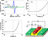 |
Fig. 1 (a) Singlet symmetrical ESR spectra of kenaf and broadleaf. (b, c) Voltagecontrolled I-V characteristics of kenaf and broadleaf, respectively. (d) Schematics of the cellulose MESFET with a recessed gate structure. |
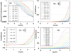 |
Fig. 2 Electronic properties of the kenaf semiconductor MESFET. (a) Id/mm–Vg characteristics of the MESFET at negative gate voltages. (b) Id–Vg characteristics of the MESFET at positive gate voltages. (c) Id/mm–Vg characteristics of the MESFET. (d) Vg dependence of Id. |
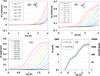 |
Fig. 3 Electronic behaviors of the broad-leaf semiconductor MESFET. Id/mm-Vd characteristics of the MESFET at (a) negative and (b) positive gate voltages. (c) Id/mm-Vg characteristics of the MESFET at positive drain voltages. (d) Id-Vg characteristics of the MESFET. |
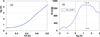 |
Fig. 4 (a) Gate voltage threshold curve versus drain voltage. (b) Id-Vg curve of cellulose MESFET at Vd = 1.4 V. |
4 Discussion
GaAs is under extensive investigation for the development of MESFETs due to their higher bandgap energies and breakdown electric fields [13,33]. Cellulose nanofibers, with similar high energy gap (4.56 eV) and large dielectric breakdown electric field (1.5 GV/cm) [34], were compared for potential future applications.
The on/off switching speed (1/τ in s–1) of the MESFET depends on the travel time (τ = W/Vd, where Vd is the drift speed) needed for electrons to move directly beneath the gate of length W. A smaller gate length and higher drift speed result in faster switching. At low energies, Vd = μe E and τ = W/μe E = W2/μe Vd [35]. For Vds = 1 V, with electron mobility μe = 55.1 cm2/Vs (Tab. 2) and W = 0.5 mm, Vd = 55.1 cm/s and τ = 18.15 μs. If a device with W = 1μm is fabricated using the nanoelectromechanical system method, Vd and τ can be determined. Table 3 provides a comparison of values for GaAs and Si [35]. As shown in Table 1, kenaf CNFs show potential as an electronic material. If hardwood CNFs can be transformed into a high-density material with fine particles, they may also likely hold promise as MESFETs in the future, similar to kenaf CNFs.
Comparison of the characteristics of kenaf, GaAs, and Si.
5 Conclusions
In this study, we measured higher carrier mobilities of 55.1 and 15.6 cm2/Vs for kenaf and broadleaf, respectively, using the Hall effect. We observed notable amplification and a higher on/off ratio in cellulose MESFETs based on the Schottky junction effect. Our results show that the CNFs can serve as a novel biomaterial FET for application in carbon-neutral electronic paper devices.
Acknowledgments
We acknowledge Editage (www.editage.jp) for providing English language editing services.
Funding
This work study received support from the research project “Cellulose Nanofiber Semiconducting Materials” under the Feasibility Study Program of the New Energy and Industrial Technology Development Organization (NEDO, 23200255-0).
Conflicts of interest
The authors declare no competing interests.
Data availability statement
The data supporting the findings of this study are available from the corresponding author upon request.
Author contribution statement
M.F. conducted the FET analysis and authored the manuscript. T. Samoto conducted the electrical measurements. K. Sakakibara synthesized kenaf CNFs. T.H. revised the paper. All authors participated in result discussions and manuscript feedback. M.F. supervised the project.
Supplementary Material
Supplementary Material is provided by the author. Access Supplementary Material
References
- M. Fukuhara, T. Yokotsuka, T. Hashida, F. Ogawa, T. Sakamoto, M. Takeda, S. Arai, A novel-n-typed semiconducting biomaterial, Sci. Rep. 12, 21899 (2022). https://doi.org/10.1038/s41598-022-26582-4 [Google Scholar]
- D. Klemm, B. Heublein, H.-P. Fink, A. Bohn, Cellulose: fascinating biopolymer and sustainable raw material, Angew. Chem. Int. Ed. 44, 3358 (2005). https://doi.org/10.1002/anie.200460587 [CrossRef] [PubMed] [Google Scholar]
- M. Fukuhara, T. Yokotsuka, S. Kayamori, A. Isogai, T. Hashida, n-Type semiconductor with energy storage made from chitosan, AIP Adv. 14, 035103 (2024). https://doi.org/10.1063/5.0188917 [Google Scholar]
- M. Fukuhara, T. Yokotsuka, N. Kobayashi, M. Kumadaki, N. Fujima, T. Hashida, Schottky-gated transistors using chitosan extracted from marine crab, Sci. Rep. 16, 1972 (2026). https://doi.org/10.1038/s41598-025-32796-z [Google Scholar]
- H. Seo, H. Matsumoto, S. Hara, M. Minagawa, A. Tanioka, H. Yako, Y. Yamagata, K. Inoue, Preparation of polysaccharide nanofiber fabrics by electrospray deposition: additive effects of poly(ethylene oxide), Polym. J. 37/6, 391 (2005) [Google Scholar]
- M. Fukuhara, T. Yokotsuka, T. Samoto, M. Kumadaki, M. Takeda, T. Hashida, Radical electron-induced cellulose-semiconductors, Sci. Rep. 14. 8692 (2024). https://doi.org/10.1038/s41598-024-59499-1 [Google Scholar]
- M. Fukuhara, T. Yokotsuka, T. Samoto, C. Saito, T. Hashida, Electronic role of biosemiconductors with C=O bonds, AIP Adv. 15, 015010 (2025). https://doi.org/10.1063/5.0235319 [Google Scholar]
- S.M. Sze, Physics of Semiconductor Devices, Chap. 5, 2nd ed. (John Wiley & Sons, New York, 1981) [Google Scholar]
- M. Fukuhara, T. Yokotsuka, T. Samoto, T. Ono, N. Fujima, T. Hashida, Characteristics of Schottky-gated field-effect transistors utilizing cellulose nano particles, AIP Adv. 15, 075047 (2025). https://doi.org/10.1063/5.0279007 [Google Scholar]
- M. Lundstrom, Physics of Nanoscale MOSFET (2008). Available at: https://nanohub.org/resources/5306 [Google Scholar]
- J.G. von Hassel, Dry Processing of GaAs-based MESFETs and Pseudomorphic HFETs, Ph.D. thesis, Eindhoven University of Technology, Eindhoven, The Netherlands, 1995. https://doi.org/10.6100/IR435811 [Google Scholar]
- Z. Fares, Y. Saidi, W. Aliouat, Effect of temperature on (I–V) statics characteristics of GaAs MESFET, J. Phys. Conf. Ser. 758, 012011 (2016). https://doi.org/10.1088/1742-6596/758/1/012011 [Google Scholar]
- N. Soni, K. Cecil, Comparative study of GaN and GaAs MESFET, Int. J. Elec. Electr. Eng. Telecom. 3, 2319 (2014). https://www.ijeetc.com/index.php?m=content&c=index&a=show&catid=157&id=974 [Google Scholar]
- S. Allen, R.S. Dadler, T. Alcorn, J. Sumakeris, R. Glass, C.H. Carter, Jr.J. Palmour, Silicon carbide MESFET’s for high-power S-band applications, Mater. Sci. Forum 264-268, 953 (1998) [Google Scholar]
- Semiconductor device, Encyclopedia Britannica, (08 September 2024), available at: https://britannica.com/technology/semiconductor-device [Google Scholar]
- H. Coskun, A. Aljabour, W. Schöfberger, A. Hinterreiter, D. Stifter, N.S. Sariciftci, P. Stadleret, Cofunction of protons as dopant and reactant activates the electrocatalytic hydrogen evolution in emeraldine-polyguanine, Adv. Mater. Interfaces 7, 1901364 (2020). https://doi.org/10.1002/admi.201901364 [Google Scholar]
- M. Fukuhara, T. Yokotsuka, T. Samoto, K. Sakakibara, N. Fujima, T. Hashida, Electronic conduction in water-absorbed kenaf cellulose, Sci. Rep. 16, 1971 (2026). https://doi.org/10.1038/s41598-025-33249-3 [Google Scholar]
- T. Samoto, T. Yokotsuka, M. Fukuhara, 3rd Research and Development Promotion Committee, Cellulose Nanofiber Semiconducting Materials, under the Feasibility Study Program of the New Energy and Industrial Technology Development Organization (NEDO, 23200255-0), 11 March 2025 [Google Scholar]
- A. Kokil, K. Yang, J. Kumar, Techniques for characterization of charge carrier mobility in organic semiconductors, J. Polym. Sci, Pt. B: Polym. Phys. 50, 1130 (2012). https://doi.org/10.1002/polb.23103 [Google Scholar]
- L. Kinder, J. Kanicki, P. Petroff, Structural ordering and enhanced carrier mobility in organic polymer thin film transistors, Synth. Met. 146, 181 (2004). https://doi.org/10.1016/j.synthmet.2004.06.024 [Google Scholar]
- T. Mikie et al., Extended π-electron delocalization in quinoid-based conjugated polymers boosts intrachain charge carrier transport, Chem. Mater. 33, 8183 (2021). https://doi.org/10.1021/acs.chemmater.1c02072 [Google Scholar]
- H. Ebata et al., Highly soluble [1]benzothieno[3,2-b]benzothiophene (BTBT) derivatives for high-performance, solution-processed organic field-effect transistors, J. Am. Chem. Soc. 129, 15732 (2007). https://doi.org/10.1021/ja074841i [Google Scholar]
- J. Takeya, M. Yamagishi, Y. Tominari, R. Hirahara, Y. Nakazawa, T. Nishikawa, T. Kawase, T. Shimoda, Very high-mobility organic single-crystal transistors withincrystal conduction channels, Appl. Phys. Lett. 90, 102120 (2007). https://doi.org/10.1063/1.2711393. [Google Scholar]
- D. Farka et al., Anderson-localization and the Mott-Ioffe-Regel limit in glassymetallic PEDOT, Adv. Electron. Mater. 3, 1700050 (2017). https://doi.org/10.1002/aelm.201700050. [Google Scholar]
- Y. Iwasa, T. Takenobu, Organic Transistors, Oyo Buturi. 77, 432 (2008) [Google Scholar]
- J.V. Li, A.M. Nardes, Z. Liang, S.E. Shaheen, B.A. Gregg, D.H. Lev, Simultaneous measurement of carrier density and mobility of organic semiconductors using capacitance techniques, Org. Electro. 12, 1879 (2011) [Google Scholar]
- S.-H. Lo, V.-P. Lee, Numerical analysis of the photoeffects in GaAs MEMFET’s, IEEE Trans. Electron Dev. 39, 1564 (1992) [Google Scholar]
- T. Jaya, V. Kannan, Analytical model for I-V characteristics of buried gate MESFET, Int. J. Adv. Sci. Technol. 17, 1 (2010) [Google Scholar]
- C. Ban et al., A universal strategy for stretchable polymer nonvolatile memory via tailoring nanostructured surfaces, Sci. Rep. 9, 10337 (2019). https://doi.org/10.1038/s41598-019-46884-4 [Google Scholar]
- I. Katsouras et al., Controlling the on/off current ratio of ferroelectric field-effect transistors, Sci. Rep. 5, 12094 (2015). https://doi.org/10.1038/srep12094 [Google Scholar]
- H. Li, R. Wang, S.-T. Han, Y. Zhou, Ferroelectric polymers for non-volatile memory devices: a review, Polym. Int. 69, 533 (2020). https://doi.org/10.1002/pi.5980 [Google Scholar]
- H. Fujimori, S. Mitani, T. Ikeda, High electrical resistivity and permeability of soft magnetic granular alloys, IEEE Trans. Mag. 30, 4779 (1994) [Google Scholar]
- V. Pala, H. Peng, P. Wright, M.M. Hella, T.P. Chow, Integrated high-frequency power converters based on GaAs pHEMT: Technology characterization and design examples, IEEE Trans. Power Electron. 27, 2644 (2012). https://doi.org/10.1109/TPEL.2011.2174803 [Google Scholar]
- M. Fukuhara et al., Amorphous cellulose nanofiber supercapacitors with voltagecharging performance, Sci. Rep. 12, 5619 (2022). https://doi.org/10.1038/s41598-022-09649-0 [Google Scholar]
- H. Hasegawa, Present status and future of GaAs high-speed device and integrated circuit technology, Jouhou Shori 25, 37 (1984) [Google Scholar]
Cite this article as: Mikio Fukuhara, Tetsuo Samoto, Keita Sakakibara, Toshiyuki Hashida, Cellulose-based metal–semiconductor field-effect transistors for paper electronics, Eur. Phys. J. Appl. Phys. 101, 8 (2026), https://doi.org/10.1051/epjap/2026004
All Tables
All Figures
|
Fig. 1 (a) Singlet symmetrical ESR spectra of kenaf and broadleaf. (b, c) Voltagecontrolled I-V characteristics of kenaf and broadleaf, respectively. (d) Schematics of the cellulose MESFET with a recessed gate structure. |
| In the text | |
|
Fig. 2 Electronic properties of the kenaf semiconductor MESFET. (a) Id/mm–Vg characteristics of the MESFET at negative gate voltages. (b) Id–Vg characteristics of the MESFET at positive gate voltages. (c) Id/mm–Vg characteristics of the MESFET. (d) Vg dependence of Id. |
| In the text | |
|
Fig. 3 Electronic behaviors of the broad-leaf semiconductor MESFET. Id/mm-Vd characteristics of the MESFET at (a) negative and (b) positive gate voltages. (c) Id/mm-Vg characteristics of the MESFET at positive drain voltages. (d) Id-Vg characteristics of the MESFET. |
| In the text | |
|
Fig. 4 (a) Gate voltage threshold curve versus drain voltage. (b) Id-Vg curve of cellulose MESFET at Vd = 1.4 V. |
| In the text | |
Current usage metrics show cumulative count of Article Views (full-text article views including HTML views, PDF and ePub downloads, according to the available data) and Abstracts Views on Vision4Press platform.
Data correspond to usage on the plateform after 2015. The current usage metrics is available 48-96 hours after online publication and is updated daily on week days.
Initial download of the metrics may take a while.