| Issue |
Eur. Phys. J. Appl. Phys.
Volume 93, Number 3, March 2021
|
|
|---|---|---|
| Article Number | 30402 | |
| Number of page(s) | 10 | |
| Section | Nanomaterials and Nanotechnologies | |
| DOI | https://doi.org/10.1051/epjap/2021200380 | |
| Published online | 11 March 2021 | |
https://doi.org/10.1051/epjap/2021200380
Regular Article
Enhancement of both optical and catalytic activity of copper-decorated porous silicon micro-particles
1
Laboratoire de Photovoltaïque, Centre de Recherches et des Technologies de l’Énergie, Technopole de Borj-Cédria, BP 95, Hammam-Lif 2050, Tunis, Tunisia
2
IEMN-DOAE- CNRS UMR 8520, Université polytechnique Hauts-de-France (UPHF), 59313 Valenciennes, France
3
Laboratory of Semi-conductors, Nano-structures and Advanced Technologies, Research and Technology Centre of Energy, Borj-Cedria Science and Technology Park, BP 95, 2050 Hammam-Lif, Tunisia
* e-mail: This email address is being protected from spambots. You need JavaScript enabled to view it.
; This email address is being protected from spambots. You need JavaScript enabled to view it.
Received:
18
December
2020
Received in final form:
4
February
2021
Accepted:
15
February
2021
Published online: 11 March 2021
Abstract
To the best of our knowledge, this study is the first to investigate the effect of chemical vapour etching (CVE) combined with copper decoration on both the optical and catalytic activities of silicon micro-particles (SiμPs). After exposure to acid vapours emanating from a hot solution of hydrogen fluoride/nitric acid (HF/HNO3), scanning electron microscope images of the treated powder show the formation of a porous, sponge-like structure on the sidewalls of SiμPs. Fourier transmission infra-red analysis shows the appearance of hydride bonds related to the formation of the porous structure. X-ray diffraction measurements and Raman spectroscopy show the good crystallinity of the samples. The strong photoluminescence properties of the obtained porous SiμPs (pSiμPs) reveal that the vapour etching process generated silicon nanocrystals within these particles. In this work, we have investigated the catalytic activity of copper nanoparticles (CuNPs) loaded on the surface of pSiμPs, in order to reduce the toxic compound 4-nitrophenol to 4-aminophenol. The results show excellent catalytic performance in very short times (less than 1 min).
© A. Hamdi et al., published by EDP Sciences, 2021
 This is an Open Access article distributed under the terms of the Creative Commons Attribution License (https://creativecommons.org/licenses/by/4.0), which permits unrestricted use, distribution, and reproduction in any medium, provided the original work is properly cited.
1 Introduction
Owing to its unique and interesting optical and electrical properties, porous silicon (abbreviated as pSi) is one of the most extensively studied semiconductors [1]. In the 1990s, the discovery of visible photoluminescence (PL) [2,3] from pSi at room temperature has motivated extensive studies. In recent years, a large effort has been made to study both the light emission origin and engineering technology of silicon micro-particles (abbreviated as SiμPs). In particular, pSi micro-particles (abbreviated as pSiμPs) were explored in diverse domains, such as in photovoltaic applications as a gettering layer, which traps undesirable impurities from metallurgical grade silicon by using different methods [4]. Chemically-modified pSiμPs have been used for sensitive and rapid humidity detection [5]. Furthermore, this porous material was used for broader applications in chemical [6] and biological sensors [7], drug delivery [8] and biomedical applications [9,10]. Moreover, many reports show that SiμPs extract hydrogen, bonded to pSi, for efficient hydrogen storage and production [11,12]. In addition, owing to its high theoretical capacity, it has been recognized as the most attractive and promising anode material for lithiumion batteries, (more than 11 times theoretical capacity of graphite) [13,14]. It has also been reported by Arafa et al. [15] that polyaniline immobilized onto metallurgical pSiμPs is highly promising for the development of an inexpensive and flexible photovoltaic system.
These types of porous micro-particles were prepared via numerous methods, such as electrochemical etching [16,17] (the most familiar method), stain-etching in a hydrofluoric acid-based solution [18,19] and by a metal-assisted chemical etching method [20,21]. Other techniques have been used to form pSi by thermal annealing and etching of silicon gels and silica nanoparticles, at 900 °C under an argon atmosphere [22,23].
However, these methods have some critical drawbacks, such as high reaction temperatures, high cost of materials, toxic reactants and low yield, limiting their large scale application [24]. So far, an inexpensive and scalable technique to produce pSiμPs represents a big challenge. The morphology of this nano-sponge material is influenced by many factors, such as the doping level of the starting material, concentration of the oxidant in the mixture, etching duration and etching temperature.
Therefore, in this paper, metallurgical grade SiμPs were selected as the feedstock, reduces the price of the raw material by nearly ten times [25]. We have studied the formation of pSiμPs via a simple and low-cost method. It is one of the cheapest approaches which acts without contacting the acid solution, since only vapour-phase etching is applied. This study was performed for the first time by Saadoun and co-workers [26], wherein pSi was produced by exposing flat silicon wafers to HF/HNO3 acid vapours. In this case, almost all procedural steps can be performed in a chemical laboratory with low-cost equipment. Recently, metal deposition onto pSi has attracted great attention in the field of catalysis. Coating of nanoparticles is an important tool that can be used to obtain different physical and chemical properties. In particular CuNPs, which are several orders of magnitude cheaper than other noble metals, were deposited on pSi and acted as a catalyst for catalytic reactions [27]. More recently, Abu Bakar et al. [28] have reported the use of pSi prepared by a stain etching method, using HF/HNO3/H2O with a ratio of (1:5:10 v/v). This pSi was used for the reduction of p-nitrophenol to p-aminophenol, which occurs within 20 min. Concerning the stability and the reusability of the catalyst, they have shown that the percentage of reduced p-nitrophenol decreased to 68% after the 4th cycle. Afterwards, they suggest the deposition of metal on pSi to enhance catalytic activity.
In this context, the surface of pSiμPs, prepared in our work using a CVE method, was loaded withCuNPs by a galvanic displacement reaction. Then, the catalytic activity of the as-prepared samplewas investigated in reduction of toxic 4-nitrophenol to 4-aminophenol, using sodium borohydride as a reducing agent. Structural and morphological characterisations of the etched and unetched samples have been performed using scanning electron microscopy/energy dispersive x-ray analysis (SEM/EDX) and X-ray diffraction (XRD) measurements, Raman, Fourier transform infra-red (FTIR) andPL spectroscopy, and UV–Vis spectrometry.
2 Experimental procedure
2.1 Chemicals
All cleaning and etching reagents were of VLSI grade. Nitric acid (HNO3, 65%) was purchased from Carlo Erba and hydrofluoric acid (HF, 48%) was supplied by BASF. Unless stated otherwise, all chemicals were reagent grade or higher. Copper (II) chloride (CuCl2), acetone, ethanol (99.5%), 4-nitrophenol and sodium borohydride (NaBH4) were purchased from Sigma-Aldrich and used as-received. Purified water (18.2 MΩcm−1 resistivity) was used for all preparations and for all rinses.
2.2 Sample preparation
2.2.1 Chemical engineering of SiμPs
Figure 1 represents the schematic illustration of the experimental chemical vapour etching setup used in this work. Indeed, commercial metallurgical-grade SiμPs were used in this work as a starting material. In the first step, 0.5 g of the dark-grey SiμPs were weighed, and ultrasonically cleaned in acetone, ethanol and ultrapure water for 10 min in sequence. The cleaned micro-particles were then dried at 60 °C overnight. In the second step, a 100 ml polypropylene container was filled with two-thirds of its volume with HF/HNO3 solution. Then, the micro-particles were dispersed in the bottom of a plastic holder. This holder was transferred into the container filled with the acid solution HF/HNO3, and placed on the top of this mixture. Finally, the container was closed and placed on a hot plate.
In this work, we used a mixture of acids containing a 48% of Hydrofluoricacid (HF) and 65% of Nitricacid (HNO3). The HF/HNO3 volume ratio was fixed at 3/1,based on the previous work of Amri et al. [29].
In order to obtain more vapor inside the container, the acid mixture was heated at 80 °C. The etching duration was 30 min (sample named CVE30). Subsequently, the etched silicon micro-particles were rinsed in DI water and dried in 60 °C oven overnight.
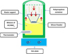 |
Fig. 1 Schematic illustration of the experimental CVE setup. |
2.2.2 Deposition of copper nanoparticles on pSiμPs
CuNPswere deposited on the surface of pSiμPs using a galvanic reaction. This was performed by dipping the SiμPs into an aqueous solution of CuCl2 (0.015 M)/HF (1.8 M), for 5 min at ambient conditions. Afterwards, the as-prepared samples were centrifuged and washed repeatedly with DI water. Finally, the resulting micro-particlesweredried at 55 °C in an oven.
2.3 Catalytic reduction of 4-nitrophenol
4-nitrophenol, a model toxic substance, was prepared in DI water at 0.1 M as a stock solution. Then, NaBH4 (200 µL, 0.1 M) was mixed with freshly-prepared aqueous solution of the hazardous compound (0.1 mM). For the reduction step, the CuNPs decorated pSiμP catalyst was added to the previous mixture. After addition, the solution was carefully mixed by shaking it gently. At the end of the reaction, the solution was taken out and filtered to remove the catalyst. Therefore, 2 cm3 quartz cuvette containing the filtered solution of 4- nitrophenol was transferred into the UV-Vis spectrophotometer to measure its absorption. To monitor the reduction of this compound, the absorption band centred at 400 and 298 nm corresponding to 4-nitrophenolate ions and 4-aminophenol, respectively was followed.
2.4 Sample characterisation
2.4.1 SEM
The morphology of SiμPs before and after acid vapour etching was characterised using an electron microscope (JEOL JSM-5400,JEOL Ltd., Akishima-shi, Japan).
2.4.2 FTIR spectroscopy
FTIR spectra were taken using a Nicolet MAGNA-IR 560 Spectrometer in the infrared region 500–4000 cm−1.
2.4.3 XRD measurements
XRD patterns were collected using a Bruker X-ray diffractometer, with Cu-Kα radiation at room temperature. X-rays were generated at 40 kV and 30 mA, with a scan speed of 1.2 min−1. The X-ray wavelength was 0.15406 nm.
2.4.4 PL spectroscopy
Photoluminescence spectra were collected using a (HR250) Jobin-Yvon spectrometerat ambient temperature, with a 4765 Å laser.
2.4.5 Raman spectroscopy
Raman spectra were measured at room temperature using a laser excitation line of 488 nm (laser power 5 mW).
2.4.6 UV–Vis spectrometry
UV–vis absorption measurements were recorded using a Perkin Elmer Lambda UV–vis 950 spectrophotometer,with a 1.0 cm quartz cuvette.
3 Results and discussion
3.1 Grain size distribution of SiμPs
Before any treatment, the particle size distribution of the initial micro-particles was measured using a Malvern Instruments Mastersizer 2000 (Malvern Instruments, Malvern, UK), using the laser scattering method. As represented in Figure 2, the measurements show that the size distribution of the starting SiμPs ranges from 1 to 140 μm. It is clear that the distribution is not uniform, and can be divided into three distinct populations belonging to three areas: the first population ranges from 1 to 15 μm, the second is between 15 and 40 μm and the third is from 40 to 140 μm. We note that the powder is composed of micro-particles, with most of them belonging in the third area, ranging from 40 to 140 μm.
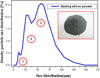 |
Fig. 2 Particle size distribution of SiμPs (insert shows a photograph of the starting micro-particles). |
3.2 Morphological characterisation
As depicted in the SEM image in Figure 3, the SiμPs have a large size distribution, confirming the previous results from the grain size distribution analysis (Sect. 3.1). The insert corresponds to the SEM image of the micro-particles at high magnification, and shows a smooth surface without pores.
After CVEfor 30 min, the formation of a porous thin layer distributed over the entire surface of the micro-particlescan be clearly observed (Fig. 4). It can also be observed that CVE of the particles occurs homogeneously on all facets. The image in the insert is a magnification of the image in Figure 4, which clearly shows that the pSiμPs have a pore diameter below 50 nm. These micro-particles retain their polyhedralmorphology, and contain a clear sponge-like structure. The formation of a porous layer on the micro-particle sidewalls may be rapidly confirmed by the change in colour, from dark-grey to black, and by the orange emission under UV illumination.
The chemical vapour etching method is used to generate porous structure. Indeed, the etching mechanism occurs via two steps [30]. Briefly, in the first step, the surface of silicon microparticles is oxidized after exposure to nitric acid (HNO3), which produce a thin silicon-oxide layer (SiO2) as described by the following chemical reaction: (1)
(1)
The second step is the dissolution of the formed SiO2 layer by HF vapors. This reaction produces a highly water-soluble H2SiF6 product, leading to a porous structure as described by the following reaction: (2)
(2)
The chemical products resulting from these two reactions are confirmed by FTIR analysis as shown in the next section.
 |
Fig. 3 SEM image of untreated SiμPs (insert image is a high-magnification view). |
 |
Fig. 4 SEM image of the pSiμPs (inserted image is a high-magnification view). |
3.3 FTIR analysis
Figure 5 shows typical FTIR absorption spectra corresponding to SiμPs before and after CVE for 30 min. For both samples, the presence of large peak at 1090 cm−1 is noted, which corresponds to the Si-O-Si asymmetric stretching mode [31]. After CVEtreatment, a considerable surface chemical modification was observed. Noteworthy are the appearance of bands which correspond to the three mainproducts resulting from the etching reaction between the silicon surface and the acid vapour: N-H4 +, N-H and SiF6 2- species, localised at 1410, 3170 cm−1 and 747; 485 cm−1, respectively. In the low-energy region, the appearance of Si-H2 in bending mode was detected, localised at 614 cm−1. These bonds are characteristic of the CVE method performed with HF/HNO3 solution, confirming the porosification of the powder.
 |
Fig. 5 FTIR absorption spectra of SiμPs before and after CVE treatment. |
3.4 PL analysis
Figure 6 exhibits the PL spectra of untreated and treated SiμPs, recorded in the range of 2.25–2.40 eV at room temperature. Untreated SiμPs do not show any PL emission, likely due to the absence of a confined structure on their sidewalls. After CVE treatment, a significant gaussian PL peak localised at 2.32 eV is detected. L.T. Canham et al. [32] have shown in their quantum confinement model that the appearance of a PL peak is attributed to the formation of silicon nanocrystallites (SiNCs), smaller than the free exciton box size. On the other hand, FTIR analysis shows that the porous micro-particle surface is partially passivated by Si-H2 and Si-O-Si bands. These two bands can create new electronic states in the band gap of the SiNCs, acting as localised states of the excited electron hole pairs. In this case, recombination in SiNCs proceeds through carriers trapped in oxygen-related localised states which are stabilized by the widening of the gap.
The crystallite size may be evaluated from the PL peak position of the treated SiμPs, according to the following equation: (3)
(3)
where E0 = 1.17 eV (band gap of bulk Si), E corresponds to the position of the peak in the PL spectrumand d is the size of the nanocrystallite [30]. Using this empirical formula, the crystallite size is 2.3 nm.
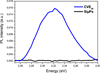 |
Fig. 6 Room-temperature PL spectra of SiμPs before and after CVE treatment. |
3.5 Raman analysis
The spectrum of SiμPs exposed to acid vapour for 30 min is similar to that of untreated silicon, as shown in Figure 7. Three major peaks are clearly observed in the 250–1000 cm−1 range. The most intense central peak corresponds to the first-order phonon mode, situated around 519.6 cm−1. On either side of the central peak, we observe two less intense peaks related to the second-order Raman spectra, implicating two phonons. The wide peak from 920 to 990 cm−1 originates from the second-order Raman band of crystalline Si–Si vibrations [33].
After CVE treatment, the principal peak exhibits an enhancement in Raman intensity. Compared with the untreated SiμPs, Raman measurements on porous micro-particles exhibit an enhancement of the first-order longitudinal optical (LO) mode peak intensities, as shown in Figure 8. This is mainly attributed to the generation of the porous layer. Raman intensity may be affected by the porosity, SiNC density or photon penetration length in the material. In addition, a shift of this mode to lower energy, from 519.8 to 516.2 cm−1, was observed. This red shift is indicative of the phonon confinement effect, due to the formation of confined nanocrystallites on the SiμPs' sidewalls.
The size of SiNC scan be estimated by this shift in the Raman peak, using the following analytical equation [34]: (4)where Δw (D) is the Raman peak shift compared to monocrystalline silicon,and D is the crystallite size. α is the lattice constant of silicon (0.543 nm), A = 47.41 cm−1 and γ = 1.44, all of which are fitting parameters that explain the phonon confinement in nanometric spheres. The crystallite size estimated from this method was 3.25 nm.
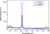 |
Fig. 7 Raman spectra of SiμPs before and after CVE treatment. |
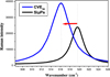 |
Fig. 8 First-order Stokes Raman spectra of SiμPs before and after CVE treatment. |
3.6 XRD measurements
XRD was used to inspect the crystallographic structure of the treated and untreated SiμPs. As depicted in Figure 9, the samples show similar and well-defined peaks, indicating the good crystallinity of the material. It is noted that the micro-particles are polycrystalline, and presented facets with different crystallographic orientations [35]. The main surface facets present in the micro-particles were (111), (200), (220) and (311) planes. From X-ray analysis, it can clearly be seen that the crystallites have preferential orientation along the (111) plane. This strong peak at 2θ = 28.65° indicates the higher population of silicon (111) [25]. This peak is broader than the same peak for untreated silicon, confirming the formation of pores on the silicon surface. Therefore, this slight broadening may be due to the formation of SiNCs after the etching process, as supported by the results of PL and Raman analysis.
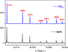 |
Fig. 9 XRD patterns of treated and untreated SiμPs. |
3.7 Reduction of 4-nitrophenol to 4-aminophenol
Firstly, copper nanoparticles were loaded on pSiμPs. As can be seen in Figure 10, the CuNPs were successfully deposited homogeneously on all facets of the porous micro-particles. The nanoparticles are deposited uniformly and are not agglomerated.
The EDX spectrum in Figure 11 showed the presence of Si, Cu, O and F. This result is consistent with the presence of copper on the surface of pSiμPs. To further confirm deposition of the CuNPs, EDX mapping analysis was performed (Fig. 12). The mapping image of Si-K, Cu-L and O-K was well-defined with sharp contrast, confirming that the CuNPs have been successfully deposited on the surface of the micro-particles.
We investigated the catalytic activity of the prepared CuNPs/pSiμPs toward the reduction of 4- nitrophenolto 4-aminophenol,in the presence of NaBH4. The catalytic reduction was followed by UV-Vis spectroscopy. After addition of NaBH4 to 4-nitrophenol solution, it was observed that the absorption peak is shifted to 400 nm. Moreover, the color changes from light yellow to yellow-green. This displacement and this color change are due to the formation of nitrophenolate ion [36], while 4-nitrophenol absorbs at 315 nm (Fig. 13). After addition of CuNPs/pSiμP catalyst to the solution, the color changes from yellow-green to colourless. The peak at 400 nm disappears within 50 s, with the appearance of a new peak at 298 nm due to the formation of 4-aminophenol.
In the literature, the catalytic reduction of this nitroaromatic compound can be described by general mechanism of heterogeneous catalysis [37,38]. In this work, this reduction occurs on the copper surface. Therefore, a plausible schematic for the reaction mechanism is represented in Figure 14. Adding NaBH4 to 4-nitrophenol increases the pH of the solution, resulting in the deprotonation of nitrophenols to nitrophenolate ions. The first step of this process is the diffusion and adsorption of hydride species (BH4 −) and 4-nitrophenol on the catalyst surface via nitro group (g–O–N=O). In the second step, the electron transfer from BH4 − (donor) to 4- nitrophenol(acceptor) occurred which allow the desorption of 4-aminophenol from the surface.
Using the same sample, 5 successive cycles of the catalytic reduction of 4-nitrophenol were performed, to evaluate the stability and reusability of the CuNPs/pSiμPs catalyst (Fig. 15).
It can be clearly seen that, after each cycle, the repeated tests did not affect the reduction activity of the catalyst; it continues to have high catalytic performance. This experiment confirms the stability and the reusability of the CuNPs/pSiμPs catalyst, during the catalytic reduction of 4-nitrophenol.
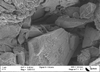 |
Fig. 10 SEM image of CuNPs-decorated pSiμPs. |
 |
Fig. 11 EDX spectrum of CuNPs-decorated pSiμPs. |
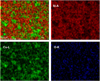 |
Fig. 12 EDX mapping of CuNP-decorated pSiμPs. |
 |
Fig. 13 UV–Vis absorption spectra during the reduction of 4-nitrophenol by NaBH4 catalysed by CuNPs/pSiμPs, over a time period of 50 s. |
 |
Fig. 14 The mechanism of reduction of 4-nitrophenol by NaBH4 in the presence of CuNPs/pSiμP catalyst. |
 |
Fig. 15 Stability of the CuNPs/pSiμPs catalyst after 5 cycles. |
4 Conclusion
In summary, metallurgical grade pSiμPs were synthesised via CVE technique, using a mix of HF/HNO3. SEM images showedthat the surface of the micro-particles after chemical etching is porous, compared to the unetched surface, and the pSiμPs have a nano-sponge-like structure. XRD was selected to study the changes in the crystal structure caused by the CVE processes, and showed that SiμPs were polycrystalline, with one facet having several crystallographic orientations. Raman spectroscopy confirmed that porous micro-particles still retain crystallinity. FTIR spectroscopy analysis illustrated that the pSiμPs contained SiF6 2- and NH4 + ions. We conclude that the CVE process does not affect the material. Finally, it was found that the as-prepared CuNPs/pSiμPs sample exhibited excellent catalytic performance in reducing 4-nitrophenol to 4-aminophenolwithin 50 s. We believe that this material may be an effective and stable catalyst for the reduction of a toxic pollutant.
Acknowledgments
This work was supported by the Ministry of Higher Education, Scientific Research and Technology of Tunisia and the Université Polytechnique Hauts-de-France (UPHF).
Author contribution statement
All the authors have participated in the preparation of the manuscript. They have read and approved the final manuscript.
References
- S. Polisski, B. Goller, A. Lapkin, D. Kovalev, ECS Trans. 16 , 69 (2008) [Google Scholar]
- L.T. Canham, Appl. Phys. Lett. 57 , 1046 (1990) [Google Scholar]
- K.B. Sundaram, J. Alizadeh, S. Albin, J. Zheng, A. Lavarias, J. Mater. Sci.-Mater. Electron. 9 , 271 (1998) [Google Scholar]
- T.E. Bell, P.T.J. Gennissen, D. DeMunter, M. Kuhl, J. Micromech. Microeng. 6 , 361 (1996) [Google Scholar]
- T. Jalkanen, E. Mäkilä, A. Määttänen, J. Tuura, M. Kaasalainen, V.-P. Lehto, P. Ihalainen, J. Peltonen, J. Salonen, Appl. Phys. Lett. 101 , 263110 (2012) [Google Scholar]
- S.D. Alvarez, A.M. Derfus, M.P. Schwartz, S.N. Bhatia, M.J. Sailor, Biomaterials 30 , 26 (2009) [PubMed] [Google Scholar]
- E.J. Anglin, L. Cheng, W.R. Freeman, M.J. Sailor, Adv. Drug Delivery Rev. 60 , 1266 (2008) [Google Scholar]
- M. Kilpeläinen, J. Riikonen, M.A. Vlasova, A. Huotari, V.P. Lehto, J. Salonen, K. H. Herzig, K. Järvinen, J. Controlled Release 137 , 166 (2009) [Google Scholar]
- E.C. Wu, J.-H. Park, J. Park, E. Segal, F. Cunin, M.J. Sailor, ACS Nano 2 , 2401 (2008) [Google Scholar]
- M. Wang, P.S. Hartman, A. Loni, L.T. Canham, J.L. Coffer, Silicon 8 , 525 (2016) [Google Scholar]
- P. Rivolo, F. Geobaldo, M. Rocchia, G. Amato, A.M. Rossi, E. Garrone, Phys. Status Solidi A 197 , 217 (2003) [Google Scholar]
- S. Litvinenko, S. Alekseev, V. Lysenko, A. Venturello, F. Geobaldo, L. Gulina, G. Kuznetsov, V. Tolstoy, V. Skryshevsky, E. Garrone, Int. J. Hydrogen Energy 35 , 6773 (2010) [Google Scholar]
- H. Wu, Y. Cui, Nano Today 7 , 414 (2012) [Google Scholar]
- Z. Jiang, C. Li, S. Hao, K. Zhu, P. Zhang, Electrochim. Acta 115 , 393 (2014) [Google Scholar]
- I.M. Arafa, H.M. El‐Ghanem, A.L. Ahmad, Polym. Int. 62 , 1283 (2013) [Google Scholar]
- M. Ohmukai, M. Taniguchi, Y. Tsutsumi, Mater. Sci. Eng., B 86 , 26 (2001) [Google Scholar]
- R.S. Dariani, Z. Ahmadi, Optik 124 , 5353 (2013) [Google Scholar]
- É. Vázsonyi, E. Szilágyi, P. Petrik, Z.E. Horváth, T. Lohner, M. Fried, G. Jalsovszky, Thin Solid Films 388 , 295 (2001) [Google Scholar]
- C.M.A. Ashruf, P.J. French, P. Bressers, J.J. Kelly, Sens. Actuators Phys. 74 , 118 (1999) [Google Scholar]
- R. Chakraborty, R. Das, J. Opt. 43 , 350 (2014) [Google Scholar]
- A.G. Cullis, L.T. Canham, P.D.J. Calcott, J. Appl. Phys. 82 , 909 (1997) [Google Scholar]
- H. Kim, B. Han, J. Choo, J. Cho, Angew. Chem. 120 , 10305 (2008) [Google Scholar]
- Z. Bao, M.R. Weatherspoon, S. Shian, Y. Cai, P.D. Graham, S.M. Allan, G. Ahmad, M.B. Dickerson, B.C. Church, Z. Kang, Nature 446 , 172 (2007) [CrossRef] [PubMed] [Google Scholar]
- Z. Zhang, Y. Wang, W. Ren, Q. Tan, Y. Chen, H. Li, Z. Zhong, F. Su, Angew. Chem. 126 , 5265 (2014) [Google Scholar]
- R. Ouertani, A. Hamdi, C. Amri, M. Khalifa, H. Ezzaouia, Nanoscale Res. Lett. 9 , 574 (2014) [PubMed] [Google Scholar]
- M. Saadoun, N. Mliki, H. Kaabi, K. Daoudi, B. Bessaıs, H. Ezzaouia, R. Bennaceur, Thin Solid Films 405 , 29 (2002) [Google Scholar]
- S. Amdouni, Y. Coffinier, S. Szunerits, M.A. Zaïbi, M. Oueslati, R. Boukherroub, Semicond. Sci. Technol. 31 , 014011 (2015) [Google Scholar]
- N.A. Bakar, A. Ridzwan, W.L. Tan, M.A. Bakar, N.A. Sabri, Mater. Chem. Phys. 232 , 387 (2019) [Google Scholar]
- C. Amri, R. Ouertani, A. Hamdi, R. Chtourou, H. Ezzaouia, Mater. Des. 111 , 394 (2016) [Google Scholar]
- C. Amri, R. Ouertani, A. Hamdi, H. Ezzaouia, Superlattices Microstruct. 91 , 278 (2016) [Google Scholar]
- C. Hong, H. Kim, H.W. Kim, C. Lee, Met. Mater. Int. 16 , 311 (2010) [Google Scholar]
- L.T. Canham, Phys. Status Solidi B 190 , 9 (1995) [Google Scholar]
- H.-H. Kim, J.-I. Son, H.-S. Yun, N.-H. Cho, Met. Mater. Int. 20 , 1115 (2014) [Google Scholar]
- İ. Doğan, M.C. van de Sanden, J. Appl. Phys. 114 , 134310 (2013) [Google Scholar]
- A. Goyal, P.R. Soni, J. Mater. Sci.-Mater. Electron. 28 , 14720 (2017) [Google Scholar]
- M.Y.A. Halim, W.L. Tan, N.H.H.A. Bakar, M.A. Bakar, Materials 7 , 7737 (2014) [Google Scholar]
- K. Sravanthi, D. Ayodhya, P.Y. Swamy, Mater. Sci. Energy Technol. 2 , 298 (2019) [Google Scholar]
- N. Berahim, W.J. Basirun, B.F. Leo, M.R. Johan, Catalysts 8 , 412 (2018) [Google Scholar]
Cite this article as: Abderrahmane Hamdi, Chohdi Amri, Rachid Ouertani, Elhadj Dogheche, Hatem Ezzaouia, Enhancement of both optical and catalytic activity of copper-decorated porous silicon micro-particles, Eur. Phys. J. Appl. Phys. 93, 30402 (2021)
All Figures
|
Fig. 1 Schematic illustration of the experimental CVE setup. |
| In the text | |
|
Fig. 2 Particle size distribution of SiμPs (insert shows a photograph of the starting micro-particles). |
| In the text | |
|
Fig. 3 SEM image of untreated SiμPs (insert image is a high-magnification view). |
| In the text | |
|
Fig. 4 SEM image of the pSiμPs (inserted image is a high-magnification view). |
| In the text | |
|
Fig. 5 FTIR absorption spectra of SiμPs before and after CVE treatment. |
| In the text | |
|
Fig. 6 Room-temperature PL spectra of SiμPs before and after CVE treatment. |
| In the text | |
|
Fig. 7 Raman spectra of SiμPs before and after CVE treatment. |
| In the text | |
|
Fig. 8 First-order Stokes Raman spectra of SiμPs before and after CVE treatment. |
| In the text | |
|
Fig. 9 XRD patterns of treated and untreated SiμPs. |
| In the text | |
|
Fig. 10 SEM image of CuNPs-decorated pSiμPs. |
| In the text | |
|
Fig. 11 EDX spectrum of CuNPs-decorated pSiμPs. |
| In the text | |
|
Fig. 12 EDX mapping of CuNP-decorated pSiμPs. |
| In the text | |
|
Fig. 13 UV–Vis absorption spectra during the reduction of 4-nitrophenol by NaBH4 catalysed by CuNPs/pSiμPs, over a time period of 50 s. |
| In the text | |
|
Fig. 14 The mechanism of reduction of 4-nitrophenol by NaBH4 in the presence of CuNPs/pSiμP catalyst. |
| In the text | |
|
Fig. 15 Stability of the CuNPs/pSiμPs catalyst after 5 cycles. |
| In the text | |
Current usage metrics show cumulative count of Article Views (full-text article views including HTML views, PDF and ePub downloads, according to the available data) and Abstracts Views on Vision4Press platform.
Data correspond to usage on the plateform after 2015. The current usage metrics is available 48-96 hours after online publication and is updated daily on week days.
Initial download of the metrics may take a while.