| Issue |
Eur. Phys. J. Appl. Phys.
Volume 87, Number 3, September 2019
|
|
|---|---|---|
| Article Number | 31001 | |
| Number of page(s) | 7 | |
| Section | Instrumentation and Metrology | |
| DOI | https://doi.org/10.1051/epjap/2019190122 | |
| Published online | 08 November 2019 | |
https://doi.org/10.1051/epjap/2019190122
Regular Article
Low temperature two STM tip tunneling measurements of a floating chemical potential Pb(111) surface
1
CEMES, Université de Toulouse, CNRS, 29 Rue J. Marvig, BP 94347, 31055 Toulouse Cedex, France
2
International Center for Materials Nanoarchitectonics (WPI-MANA), National Institute for Materials Science (NIMS), Namiki, Tsukuba, Ibaraki 305-0044, Japan
* e-mail: This email address is being protected from spambots. You need JavaScript enabled to view it.
Received:
10
April
2019
Received in final form:
4
September
2019
Accepted:
1
October
2019
Published online: 8 November 2019
Abstract
On a Pb(111) superconducting surface, low temperature dI/dV tunnelling spectra are recorded between two scanning tunnelling microscopes (STM) metallic tips with the Pb(111) sample metallic support non-grounded. The tunnelling current intensity I passing between the 2 tips through the sample is controlled by changing one or both STM vacuum tunnelling junction resistances. The chemical potential of this floating Pb(111) surface depends on the normalized ratio between those two quantum resistances. When ungrounded, the Pb(111) sample chemical potential balances between those of the 2 STM tips while tuning their respective tip end atomic apex to Pb(111) surface distances with a picometer precision without any physical contact between the STM tips and the surface.
© W.-H. Soe et al., EDP Sciences, 2019
 This is an Open Access article distributed under the terms of the Creative Commons Attribution License (http://creativecommons.org/licenses/by/4.0), which permits unrestricted use, distribution, and reproduction in any medium, provided the original work is properly cited.
1 Introduction
In a multiple contact electrodes set–up fabricated on the surface of a conductive material to characterize, for example, its intrinsic electronic transport properties, the different chemical potentials of the source, drain and/or floating electrodes are governing the current intensities passing through the sample [1]. Current intensities also depend on the contact resistances (Ballistic, Ohmic, Schottky) between the electrodes and the sample, especially when the sample size is smaller than the electronic mean free path of the material [1,2]. The contact electrodes are usually fabricated using micro and nanofabrication techniques [3]. Their positioning onto the sample surface is fixed (one multiple contacts configuration per fabrication run) and located at best with a few nanometres precision on this surface [4,5]. The precision is generally less due to the lateral diffusion of the very last metal atoms during the electrodes metallization step [6] either using a resist, a shadow mask [7,8] or a dynamic stencil [9].
Recently, multi-probes scanning tunnelling microscopes (STM) have been developed to enable a movable and more precise way of positioning the contacting electrodes. Here and on the sample surface, the lateral and vertical positioning of the STM tip electrodes is controlled within a few nanometers. More important, the contact resistances can be adjusted using the STM tip-to-surface vertical distance [10–14]. Without touching physically the surface, it opens the way to control the elementary electron transfer processes from the tip end apex to the sample surface (or the reverse) at the origin of the measured tunnelling current intensity.
Such a tunnelling contact is obtained when the STM tip end atom is maintained further away from the surface uppermost atom than the van der Walls distances. There is no physical deformation of the surface nor chemical bond to the surface. In this case and when the sample is not grounded, its surface is set in an electronic floating configuration with still electrons able to be transferred from one STM tip to another through the surface. In this configuration explored below, there is a non-classical potential drop due to decoherence effects at each tip apex to surface vacuum tunnelling junction. This strictly non-invasive measurement configuration is to be found when the electronic orbitals overlap between the sample surface and the STM end atom tip apex are maintained as small as possible while conserving long range electron transfer events between the tips through the surface. This configuration is also to be found when measuring the intrinsic conductance of a surface atomic wire [15] or a molecular wire [16] without perturbing their molecular orbitals [17].
To reach this strictly non-invasive tunnelling measurement configuration, a new very stable low temperature (LT) ultra-high vacuum (UHV) four STM scanners instrument (LT-UHV 4-STM) [18] is used to measure the chemical potential of an atomically clean UHV prepared Pb(111) sample in a 2 + 1 contacts configuration. The 2 contacts are non-invasive tunnelling contacts as defined above and the third one is a macroscopic very low ohmic contact resistance at the back of the Pb(111) sample. The first electrode (the source, Tip A) is one atom sharp STM tip apex of the LT-UHV 4-STM. It is not physically nor electronically touching the surface. Using an external voltage source, it is maintained at a well-controlled electronic chemical potential μA = EF + eVA where EF is the tip metal material electronic Fermi level. The second electrode (the drain, Tip B) is a second STM tip apex (Tip B) of the same instrument. It is also not touching the surface and set at a well-controlled chemical potential μB = EF + eVB . The third electrode is static: the underlying stainless steel Pb(111) sample holder on the LT-UHV 4-STM. This holder can be automatically and in situ connected to (or disconnected from) a well-defined macroscopic ground as discussed formally in [19]. When not grounded, the “lead-stainless steel bulk” chemical potential μS is floating between μA and μB. As measured in this paper, µS depends critically on the atomic scale Tip A and Tip B vacuum tunnelling contacts resistance to the Pb(111) surface. We demonstrate how µS can be tuned in real time by setting the two STM tips distance from the Pb(111) surface with a few picometers precision on our LT-UHV 4-STM required to master those non-invasive tunnel contacts.
2 Preparation of the floating two tips surface measurements
The clean Pb(111) surface of the lead sample mounted on its stainless steel holder was prepared following a multiple cycles of Ar+ surface sputtering and 160 °C annealing in the UHV preparation chamber of our Scienta-Omicron low temperature LT-UHV 4-STM [18]. The Pb(111) sample was transferred in UHV onto the sample stage and cooled down to liquid helium (LHe) temperature, below the superconducting transition temperature of lead (Tc = 7.19 K). The superconducting Pb(111) surface was preferred to a standard non-superconducting metal surface to follow the zA variations using the well characterized Pb(111) superconducting gap observable in dI/dV curves.
A typical LT-UHV STM image recorded using one scanner of our LT-UHV 4-STM is presented in Figure 1a. The dark hexagonal features originate from the quantum well electronic states created between the topmost Pb(111) surface and the sub-surface Ar bubbles formed during the Pb(111) surface preparation [20]. The preparation of the atomic scale STM tip apex with a single end atom was performed by a soft indentation in the Pb(111) surface of each STM tip before the measurements (Fig. 1b). At LHe temperature, it certainly results in a wetting of the tungsten tip apex with a few Pb atoms. All our tunnelling junctions formed by this gentle indentation are still superconducting-vacuum-normal metal junctions, the lead layer thickness captured during the tip indentation remaining at the atomic scale. The dI/dV spectrum of such a junction is presented in Figure 1c with the Pb(111) sample macroscopically back grounded through the sample holder. It demonstrates a clear superconducting gap which is reproducible with all tips on the LT-UHV 4-STM and on any atomically flat terrace of the Pb(111) surface. According to this measurement, an effective 6 K tunnel junction temperature can be estimated [21].
Since the 4 STM tips of our multi-probes LT-UHV can be controlled and scanned independently on the same Pb(111) surface, Tip B was first set in a ballistic contact transport regime and Tip A in a tunnelling contact regime with the Pb(111) sample surface. To achieve this configuration, the distance zB between the end atom of the Tip B apex and the Pb(111) surface was first fine-tuned to reach one quantum of resistance (RB = 12.9 kΩ). This was performed using the current-distance characteristics IB(zB) recorded by anticipation with the sample holder still grounded as presented in Figure 1d, leading to a 3.45 eV apparent tunnel barrier height [22]. This IB(zB) curve illustrates the stability of our instrument in mastering the tip apex end atom to surface distance > 0.06 nm with a precision better than 2 pm (see Ref. [18]) for mastering a strictly non-invasive vacuum tunnelling contact per tip. Then, this holder was disconnected from the ground with a Tip A tunnelling junction resistance RA ≫ 12.9 kΩ. The fine-tuned contact resistance of Tip B was preserved by freezing zB, which is possible thanks to the stability of our LT-UHV 4-STM (lateral stability: <0.9 nm per hour [18]). Its chemical potential µB was controlled by shifting the virtual ground of its STM I–V converter from zero to VB = +/–30 mV (Fig. 2b). Since RB = 12.9 kΩ, this is also fixing the Pb(111) surface chemical potential to µB (see below). Tunnelling dI/dV spectra were recorded with Tip A still in a tunnelling contact junction mode on the Pb(111) surface. As presented in Figure 2b, indeed a µB change by +/–30 mV shifts the dI/dV spectra accordingly with no deformation. The Tip A to Tip B apex distance can be as large as 6 mm on our instrument with no voltage drop along the superconducting Pb(111) surface while scanning Tip A with an immobile Tip B. Such dI/dV recording certifies that the virtual ground on the Tip B STM electronics is working perfectly through the input transistors differential pair of its I–V converter.
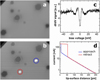 |
Fig. 1 Typical constant current Pb(111) surface images (a) before and (b) after constructing one after the other two quantum point contacts where atomic droplets have been produced while retracting the tip apex (see Fig. 1d for Tip B) with a Pb single atom (red circle) and a Pb dimer (blue circle). The hexagonal features in (a) and (b) are Ar-bubbles created during sample cleaning process in the vicinity of surface [20]. (c) Tip A dI/dV spectrum showing the superconducting gap characteristics of a superconductor-vacuum-metal junction. Notice that the bias voltage was ramped up by of steps 0.1 mV per 0.1 s for all measurements presented in this paper to avoid any low pass filter effect. (d) Two single shot current distance characteristics I(z) recorded on Tip B to determine the zB tip apex to surface relative distance to reach the 12.9 kΩ quantum contact resistance. At this quantum contact, Tip B gives IB = 183 nA for VB = 6 mV i.e. an RB = 32.8 KΩ junction resistance (12.9 kΩ + a very low noise 20 kΩ metallic resistance in series). (a) and (b) images STM: I = 10 pA, V = 30 mV, images size: 40 nm × 30 nm. Equivalent images for Tip A and Tip B. The single one shot IB = IB(zB) were recorded in 10 s with the corresponding STM B feedback loop frozen. Multiple single shot I(z) characteristics were recorded for Tip A and Tip B. They present all the same slope (work-function). Only the jump to contact is changing from curve to curve with a z shift below 50 pm. |
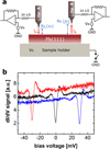 |
Fig. 2 (a) The two STM tip measurement electrical circuit diagram used on the Pb(111) surface with its 2 virtual ground I–V converters and the back ground controllable switch connected to the sample holder. TheVS sample holder is defined using µS = EF +eVS. (b) Three “one shot” dI/dV spectra recorded on Tip A while the far away Tip B is in atomic point contact with the Pb(111) surface to control the sample chemical potential from its surface. Tip B potential is VB = 0.0 mV (black), VB = +30 mV (blue) and VB = –30 mV (red). Tip A was stabilized in a tunnelling regime with its STM Feed-back loop set up IA = 200 pA, for VA = 30 mV. |
3 Two tips measurements in a sample floating mode
Starting from Tip A in tunnelling and Tip B in ballistic contact regimes, the distance zB between Tip B apex and the Pb(111) surface was systematically varied to change the Tip B junction resistance from this ballistic to different tunnelling junction resistances. With VA and VB set to 30 mV and the sample holder grounded, the STM feedback loop current was first set at IA = 200 pA for Tip A and IB = 2 nA for Tip B. Once zA and zB are stabilized, the feedback loop of both STM's are opened and the sample holder disconnected from the ground. A spectroscopic measurement is then performed by sweeping VA, while VB is set to zero (µB = EF) through its STM I–V convertor. At the end of a measure sequence, both tips and the sample are back to their initial set up and sample holder grounded with the feedback loops on. Then, the corresponding RA and RB tunnelling junction resistances are set to the next values by changing again the feedback loop current set points. As presented in Figure 3, a set of measurements correspond to the Tip B current setting reduced measurement after measurement sequences from 2 nA to 200 pA in 10 set points (2 nA, 1 nA, and down to 200 pA at intervals of 100 pA). When reaching IB = 200 pA, Tip A current was then increased from its initial IA = 200 pA up to 2 nA following an equivalent measurement sequence now on Tip A in 10 set points.
When the sample holder ground is disconnected, Tip B acts as a virtual ground. The tunnelling current flows from Tip A to Tip B through the Pb(111) sample with e(VA − VB) the Tip A to Tip B chemical potential difference. At each (IA, IB) combination of the feedback loops set points, a dIA/d VA−B spectrum was recorded on Tip A and then a dIB/d VA−B on Tip B using a standard lock-in technique on each junction. All dI/dV spectra shown in Figure 3 were recorded in constant height mode and with no averaging. For reference, Figure 3(a)i and (b)i presents respectively the dIA/dVA−GS and dIB/dVB−GS characteristics recorded independently, both in a tunnelling contact, just before disconnecting the sample holder ground. The details of the spectrum features are different from Tip A to Tip B because of different tip apex atomic scale configurations.
For the data set selectively presented Figure 3ii to Figure 3iv and with both junction bias set up at 30 mV, a pair of set point currents (IA, IB) corresponds here to a relative  resistance ratio of respectively 0.91, 0.83, 0.75, 0.60, 0.50, 0.29, 0.17, and 0.09. The dI/dV spectra were obtained between Tip A and Tip B while the µS sample holder is floating normally between µA and µB (see below). The spectrum recorded at the junction with the highest resistance, i.e., fixed at a larger tip apex to surface distance, shows an apparent superconducting gap close to the reference shown by Figure 3i (for example, the topmost spectrum for Tip A 3(a)ii and the bottom most spectrum for Tip B in 3(b)ii). On the contrary, spectra recorded from lower resistance junctions (smaller tip-sample distance) exhibit a progressively deformed dI/dV spectrum with a wider apparent superconducting gap.
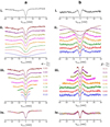 |
Fig. 3 A double selective series (a)ii and (b)ii of dI/dV spectra recorded on a Pb(111) sample non grounded when both STM Tip A and Tip B are in tunnelling conditions. For reference, the (a)i and (b)i spectra have been recorded on Tip A and Tip B with the sample grounded. The α and β parameters are obtained by fitting the (a)ii and (b)ii spectra to the (a)i and (b)i dI/dV spectra recorded independently on the Tip A and Tip B dedicated lock-in when the sample was grounded. This fitting leads to the series (a)iii and (b)iii also perfectly superposed on (a)iv and (b)iv. VA-S = (VA − VS) the voltage difference between Tip A and the sample holder floating (see Fig. 2a), V B-S = (VS − VB) between Tip B and the sample holder floating and VA-B = (VA − VB) between Tip A and Tip B. VA-GS and VB-GS are the Tip A and Tip B bias voltage when the sample holder is grounded (GS). |
4 Discussion
To understand this apparent distortion of the measured superconducting gap when the sample holder is not grounded, the conductance G = eI/(µA–µB) of the entire system constituted by the 2 tunnel junctions A, B and the Pb(111) sample, can be written [23]: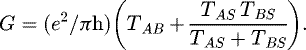 (1)
TAB is the phase coherent transport contribution giving the number of electrons per second created by the source electrode Tip A, transferred through the tunnel barrier A, travelling in the sample between two A and B junctions without energy loss, and detected directly by the drain electrode Tip B via the tunnel junction B [19]. The second term in is a phase decoherence and energy relaxation term [23] including also for a superconducting sample the copper pair breakdown process. Here, TAS
(respectively TBS
) is the transmission coefficient of the tunnelling electrons between the source electrode Tip A (resp. Tip B) and the sample through the vacuum tunnel junction A (resp. B). For this path, the transferred electrons into the superconductor sample are creating Cooper pairs at µS (i.e. losing the initial energy and phase). Those pairs are reaching the lead-stainless interface, are destructed (loosing also their phase and energy) and are absorbed by the stainless steel sample holder which is in a normal metallic state. When the sample holder is not grounded, it still acts like an electron reservoir [1,2]. Following [23], an effective chemical potential µS can be defined for this floating reservoir leading from (1) to:
(1)
TAB is the phase coherent transport contribution giving the number of electrons per second created by the source electrode Tip A, transferred through the tunnel barrier A, travelling in the sample between two A and B junctions without energy loss, and detected directly by the drain electrode Tip B via the tunnel junction B [19]. The second term in is a phase decoherence and energy relaxation term [23] including also for a superconducting sample the copper pair breakdown process. Here, TAS
(respectively TBS
) is the transmission coefficient of the tunnelling electrons between the source electrode Tip A (resp. Tip B) and the sample through the vacuum tunnel junction A (resp. B). For this path, the transferred electrons into the superconductor sample are creating Cooper pairs at µS (i.e. losing the initial energy and phase). Those pairs are reaching the lead-stainless interface, are destructed (loosing also their phase and energy) and are absorbed by the stainless steel sample holder which is in a normal metallic state. When the sample holder is not grounded, it still acts like an electron reservoir [1,2]. Following [23], an effective chemical potential µS can be defined for this floating reservoir leading from (1) to:
 (2)
(2)
At the drain electrode (Tip B) side, the detected electrons are created by the decomposition of Cooper pairs which are supplied by electrons coming both from A directly and indirectly from this holder reservoir. Notice that in Figure 3 presented measurement series, TAB was at least experimentally one order of magnitude lower than TAS and TBS . This was confirmed by measuring the IAB − VAB characteristics in the floating mode leading to G in (1) and this for different feedback set-up of the Tip A and Tip B junctions (see Fig. 4).
After having used those quantum electron transfer processes through the Pb(111) surface and the bulk to get µS, it can be of interest to define an effectiveVS using the linear relation µS = EF +eVS indicative of the sample chemical potential shift in reference to the equilibrium EF (without electron transfer through the sample). Starting first from this effective VS definition can also be considered as a reciprocal of the approach presented in [23]. Then, VA–VB can be written according to (2):
 (3)
where α =
(3)
where α =  , β =
, β =  and ideally α + β = 1. In Figure 5a, the experimental values of α and β were determined by progressively contracting (dilating) the voltage axis of the dI/dV curves presented in Figure 3 until they matched the reference Pb(111) sample holder grounded dI/dV Figure 3(a)i or (b)i spectra. The converse behavior of the spectra recorded at Tip A and Tip B results in an opposite variation of α and β with the resistance ratio. The crossing between the α and β curves does not occur exactly at 0.5. We believe that this is due to different tip apex end atomic scale structure between Tip A and Tip B. It leads to a small difference in the apparent tunnel barrier height estimated from the slope of the corresponding IA(zA) and IB(zB) curves already measured when the holder is grounded. Since the metal to metal contact between the back surface of the lead sample and the top surface of stainless steel sample holder is ohmic in our experiment, the lead sample and its holder are at the same µS equilibrium chemical potential.
As indicated above, we have also measured RA = (πħ/e 2) ×TAS −1 and RB = (πħ/e 2) ×TSB −1 independently as a function of Tip A and Tip B apex distance to the Pb(111) surface by recording their respective IA(zA) and IB(zB) characteristics when the holder was grounded. Knowing RA and RB and following (3), we can determine the VS variations based on those data sets as presented in Figure 5b. Notice that when Tip B is exactly at ballistic contact (TSB = 1 or RB = 12.9 kΩ) and TAS << 1, then VS = VB. This is consistent with the zero shift of the dI/dV spectra presented in Figure 2a for a non-zero VB.
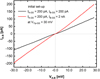 |
Fig. 4 Two examples of a direct floating IAB − VAB characteristics recorded with the 2 initial set-up indicated when the sample was grounded. After setting up Tip A and Tip B distances to the Pb(111) surface, the sample was ungrounded. For this set up and for example in the symmetric set-up case IA−GS = 200 pA, IB−GS = 200 pA at 30 mV, it comes for the direct to the ground TAS = 0.8613 × 10⁻⁴ (for sample grounded) and TBS = 0.8613 × 10⁻⁴ (for sample grounded). The total transmission coefficient (leading to G in Eq. (1) via the Landauer formula) is T = 0.4737 × 10⁻⁴ leading to TAB < 0.043 × 10⁻⁴ (sample not grounded). |
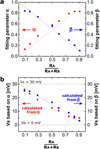 |
Fig. 5 (a) Variation of the experimental α and β obtained in (3) as a function of the |


5 Conclusion
The floating chemical potential of a lead superconducting metallic sample have been determined at LHe temperature, by transferring electrons through the Pb(111) surface of this sample between 2 STM tips (the source and the drain electrodes) in a three electrodes configuration where the end atom apex atomic orbitals of each tip are not hybridized with the ones of the uppermost Pb(111) surface atoms. The source and drain vacuum tunneling junction resistances with the Pb(111) surface were controlled by tuning the tip apex end atom distance to the Pb(111) surface with a few picometers precision. The decoherence and relaxation effects coming from those vacuum tunneling junctions and the non-superconducting metallic support of the lead sample has been demonstrated. This support is playing the role of a third electrode. Not grounded, it can be considered as an electron reservoir, the chemical potential of which can be balanced quantum mechanically between the source and drain chemical potentials by a fine tuning of the source and drain atomic scale tunneling contact resistance to the Pb(111) surface.
Authors contribution statement
We-Hyo Soe carried out the majority of the experimental work and Christian Joachim of the measurement interpretation. All authors contributed to discussions and writing manuscript. The authors thanks to Takashi Uchihashi from MANA-NIMS for constructive discussion about surface superconductivity, to Erik Dujardin and David Martrou from PicoLab at GNS-CEMES for their support during this work.
References
- M. Büttiker, Phys. Rev. B 33, 3020 (1986) [Google Scholar]
- M. Büttiker, Phys. Rev. B 35, 4123 (1987) [Google Scholar]
- R. Voss, R.B. Laibowitz, A.N. Broers, Appl. Phys. Lett. 37, 656 (1980) [Google Scholar]
- S. Washburn, IBM J. Res. Dev. 32, 335 (1988) [Google Scholar]
- R. de Piccioto, H.L. Stormer, L.N. Pfeiffer, K.W. Baldwin, K.W. West, Nature 411, 51 (2001) [CrossRef] [PubMed] [Google Scholar]
- M. Fujimori, S. Hieke, Y. Tarada, T. Hashizume, Nanotechnology 15, S333 (2004) [Google Scholar]
- T.N. Tun, M.H.T. Lwin, H.H. Kim, N. Chandrasekar, C. Joachim, Nanotechnology 18, 335301 (2007) [Google Scholar]
- T. Ushihashi, U. Ramsperger, T. Nakayama, M. Aono, Jpn. J. Appl. Phys. 47, 1797 (2008) [Google Scholar]
- S. Egger, A. Ilie, Y. Fu, J. Chongsathien, D.J. Kang, M.E. Welland, Nano Lett. 5, 15 (2005) [CrossRef] [PubMed] [Google Scholar]
- C. Joachim, D. Martrou, M. Rezeq, C. Troadec, D. Jie, N. Chandrasekhar, S. Gauthier, J. Phys: Condens. Matter. 22, 084025 (2010) [CrossRef] [PubMed] [Google Scholar]
- R. Thamankar, T.L. Yap, K.E.J. Goh, C. Troadec, C. Joachim, Appl. Phys. Lett. 103, 083106 (2013) [Google Scholar]
- J. Baringhaus, M. Ruan, F. Edler, A. Tejeda, M. Sicot, A.T. Ibrahimi, A. Ping Li, Z. Jiang, E.H. Conrad, C. Berger, C. Tagenkamp, W.A. de Heer, Nature 506, 349 (2014) [CrossRef] [PubMed] [Google Scholar]
- B. Voigtlander, V. Cherepanov, S. Korte, A. Leis, D. Cuma, S. Just, F. Lüpke, Rev. Sci. Inst. 89, 101101 (2018) [CrossRef] [Google Scholar]
- O. Kubo, Y. Shingaya, M. Nakaya, M. Aono, T. Nakayama, Appl. Phys. Lett. 88, 254101 (2006) [Google Scholar]
- M. Kolmer, P. Brandimarte, J. Lis, R. Zuzak, S. Godlewski, H. Kawai, A. Garcia-Lekue, N. Lorente, T. Frederiksen, C. Joachim, D. Sanchez-Portal, M. Szymonski, Nat. Commun. 10, 1573 (2019) [CrossRef] [PubMed] [Google Scholar]
- L. Lafferentz, F. Ample, H. Yu, S. Hetch, C. Joachim, L. Grill, Science 323, 1193 (2009) [Google Scholar]
- C. Joachim, J.K. Gimzewski, R.R. Schlittler, C. Chavy, Phys. Rev. Lett. 74, 2102 (1995) [CrossRef] [PubMed] [Google Scholar]
- J. Yang, D. Sordes, M. Kolmer, D. Martrou, C. Joachim, Eur. Phys. J. Appl. Phys. 73, 10702 (2016) [CrossRef] [EDP Sciences] [Google Scholar]
- J.M. Byers, M.E. Flatté, Phys. Rev. Lett. 74, 306 (1995) [CrossRef] [PubMed] [Google Scholar]
- M. Schmid, W. Hebenstreit, P. Varga, S. Crampin, Phys. Rev. Lett. 76, 2298 (1996) [CrossRef] [PubMed] [Google Scholar]
- S.H. Pan, E.W. Hudson, J.C. Davis, Appl. Phys. Lett. 73, 2992 (1998) [Google Scholar]
- G. Binnig, H. Rohrer, Ch. Gerber, E. Weibel, Phys. Rev. Lett. 49, 57 (1982) [Google Scholar]
- M. Büttiker, IBM J. Res. Develop. 32, 317 (1988) [CrossRef] [Google Scholar]
Cite this article as: We-Hyo Soe, Corentin Durand, Christian Joachim, Low temperature two STM tip tunneling measurements of a floating chemical potential Pb(111) surface, Eur. Phys. J. Appl. Phys. 87, 31001 (2019)
All Figures
|
Fig. 1 Typical constant current Pb(111) surface images (a) before and (b) after constructing one after the other two quantum point contacts where atomic droplets have been produced while retracting the tip apex (see Fig. 1d for Tip B) with a Pb single atom (red circle) and a Pb dimer (blue circle). The hexagonal features in (a) and (b) are Ar-bubbles created during sample cleaning process in the vicinity of surface [20]. (c) Tip A dI/dV spectrum showing the superconducting gap characteristics of a superconductor-vacuum-metal junction. Notice that the bias voltage was ramped up by of steps 0.1 mV per 0.1 s for all measurements presented in this paper to avoid any low pass filter effect. (d) Two single shot current distance characteristics I(z) recorded on Tip B to determine the zB tip apex to surface relative distance to reach the 12.9 kΩ quantum contact resistance. At this quantum contact, Tip B gives IB = 183 nA for VB = 6 mV i.e. an RB = 32.8 KΩ junction resistance (12.9 kΩ + a very low noise 20 kΩ metallic resistance in series). (a) and (b) images STM: I = 10 pA, V = 30 mV, images size: 40 nm × 30 nm. Equivalent images for Tip A and Tip B. The single one shot IB = IB(zB) were recorded in 10 s with the corresponding STM B feedback loop frozen. Multiple single shot I(z) characteristics were recorded for Tip A and Tip B. They present all the same slope (work-function). Only the jump to contact is changing from curve to curve with a z shift below 50 pm. |
| In the text | |
|
Fig. 2 (a) The two STM tip measurement electrical circuit diagram used on the Pb(111) surface with its 2 virtual ground I–V converters and the back ground controllable switch connected to the sample holder. TheVS sample holder is defined using µS = EF +eVS. (b) Three “one shot” dI/dV spectra recorded on Tip A while the far away Tip B is in atomic point contact with the Pb(111) surface to control the sample chemical potential from its surface. Tip B potential is VB = 0.0 mV (black), VB = +30 mV (blue) and VB = –30 mV (red). Tip A was stabilized in a tunnelling regime with its STM Feed-back loop set up IA = 200 pA, for VA = 30 mV. |
| In the text | |
|
Fig. 3 A double selective series (a)ii and (b)ii of dI/dV spectra recorded on a Pb(111) sample non grounded when both STM Tip A and Tip B are in tunnelling conditions. For reference, the (a)i and (b)i spectra have been recorded on Tip A and Tip B with the sample grounded. The α and β parameters are obtained by fitting the (a)ii and (b)ii spectra to the (a)i and (b)i dI/dV spectra recorded independently on the Tip A and Tip B dedicated lock-in when the sample was grounded. This fitting leads to the series (a)iii and (b)iii also perfectly superposed on (a)iv and (b)iv. VA-S = (VA − VS) the voltage difference between Tip A and the sample holder floating (see Fig. 2a), V B-S = (VS − VB) between Tip B and the sample holder floating and VA-B = (VA − VB) between Tip A and Tip B. VA-GS and VB-GS are the Tip A and Tip B bias voltage when the sample holder is grounded (GS). |
| In the text | |
|
Fig. 4 Two examples of a direct floating IAB − VAB characteristics recorded with the 2 initial set-up indicated when the sample was grounded. After setting up Tip A and Tip B distances to the Pb(111) surface, the sample was ungrounded. For this set up and for example in the symmetric set-up case IA−GS = 200 pA, IB−GS = 200 pA at 30 mV, it comes for the direct to the ground TAS = 0.8613 × 10⁻⁴ (for sample grounded) and TBS = 0.8613 × 10⁻⁴ (for sample grounded). The total transmission coefficient (leading to G in Eq. (1) via the Landauer formula) is T = 0.4737 × 10⁻⁴ leading to TAB < 0.043 × 10⁻⁴ (sample not grounded). |
| In the text | |
|
Fig. 5 (a) Variation of the experimental α and β obtained in (3) as a function of the |
| In the text | |
Current usage metrics show cumulative count of Article Views (full-text article views including HTML views, PDF and ePub downloads, according to the available data) and Abstracts Views on Vision4Press platform.
Data correspond to usage on the plateform after 2015. The current usage metrics is available 48-96 hours after online publication and is updated daily on week days.
Initial download of the metrics may take a while.