Fig. 1
Download original image
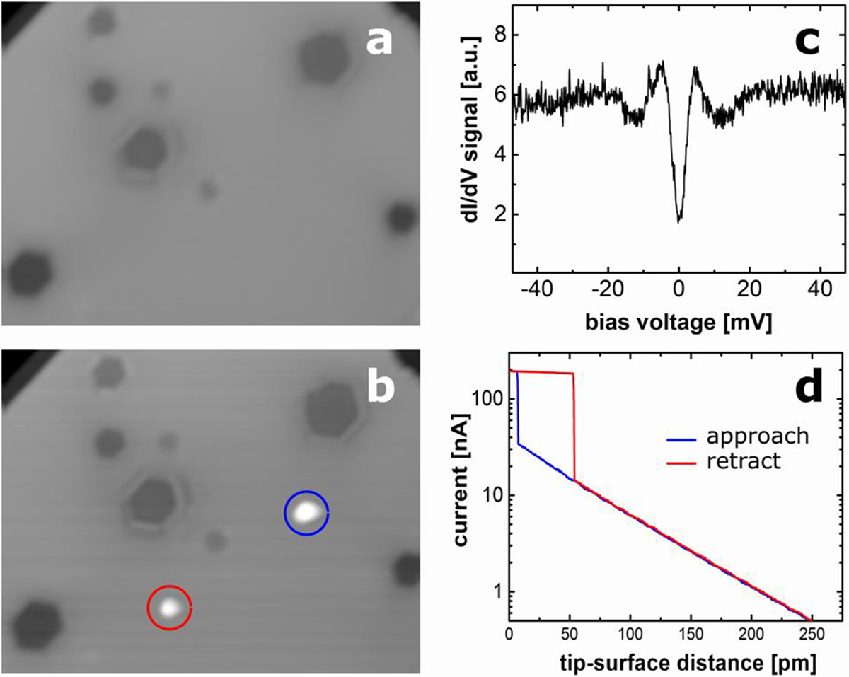
Typical constant current Pb(111) surface images (a) before and (b) after constructing one after the other two quantum point contacts where atomic droplets have been produced while retracting the tip apex (see Fig. 1d for Tip B) with a Pb single atom (red circle) and a Pb dimer (blue circle). The hexagonal features in (a) and (b) are Ar-bubbles created during sample cleaning process in the vicinity of surface [20]. (c) Tip A dI/dV spectrum showing the superconducting gap characteristics of a superconductor-vacuum-metal junction. Notice that the bias voltage was ramped up by of steps 0.1 mV per 0.1 s for all measurements presented in this paper to avoid any low pass filter effect. (d) Two single shot current distance characteristics I(z) recorded on Tip B to determine the zB tip apex to surface relative distance to reach the 12.9 kΩ quantum contact resistance. At this quantum contact, Tip B gives IB = 183 nA for VB = 6 mV i.e. an RB = 32.8 KΩ junction resistance (12.9 kΩ + a very low noise 20 kΩ metallic resistance in series). (a) and (b) images STM: I = 10 pA, V = 30 mV, images size: 40 nm × 30 nm. Equivalent images for Tip A and Tip B. The single one shot IB = IB(zB) were recorded in 10 s with the corresponding STM B feedback loop frozen. Multiple single shot I(z) characteristics were recorded for Tip A and Tip B. They present all the same slope (work-function). Only the jump to contact is changing from curve to curve with a z shift below 50 pm.
Current usage metrics show cumulative count of Article Views (full-text article views including HTML views, PDF and ePub downloads, according to the available data) and Abstracts Views on Vision4Press platform.
Data correspond to usage on the plateform after 2015. The current usage metrics is available 48-96 hours after online publication and is updated daily on week days.
Initial download of the metrics may take a while.