| Issue |
Eur. Phys. J. Appl. Phys.
Volume 98, 2023
Special Issue on ‘Advances in Renewable Energies, Materials and Technology’, edited by Laurene Tetard, Hamid Oughaddou, Abdelkader Kara, Yannick Dappe and Nabil Rochdi
|
|
|---|---|---|
| Article Number | 41 | |
| Number of page(s) | 8 | |
| Section | Nanomaterials and Nanotechnologies | |
| DOI | https://doi.org/10.1051/epjap/2023230004 | |
| Published online | 13 June 2023 | |
https://doi.org/10.1051/epjap/2023230004
Regular Article
First steps of silicene growth on an insulating thin-film: effect of the substrate temperature
1
Institut des Sciences Moléculaires d'Orsay, ISMO-CNRS, Bât. 520, Université Paris-Saclay, 91405 Orsay, France
2
Synchrotron Soleil, L'Orme des Merisiers Saint-Aubin, B.P. 48, 91192 Gif-sur-Yvette Cedex, France
3
LaMCScI, Faculté des Sciences, Université Mohammed V − Agdal, 10100 Rabat, Morocco
4
Hassan II Academy of Sciences and Technology, Rabat, Morocco
5
Department of Physics, University of Central Florida, Orlando, FL 32816, USA
6
Département de Physique, CY, Université Cergy-Pontoise, 95031 Cergy-Pontoise Cedex, France
* e-mail: This email address is being protected from spambots. You need JavaScript enabled to view it.
Received:
4
January
2023
Revised:
24
March
2023
Accepted:
12
April
2023
Published online: 13 June 2023
Abstract
Silicene is a two-dimensional (2D) material with very promising electronic properties for applications in silicon modern technology. However, the first experimental synthesis of silicene on metallic surfaces shows strong interactions between the silicene and its substrate, which can alter its electronic properties. Here, we report on the first steps of silicene growth on an insulating surface (NaCl) using scanning tunneling microscopy (STM), low energy electron diffraction (LEED), Auger electron spectroscopy (AES), and angle-resolved photoemission spectroscopy (ARPES). We demonstrate the importance of temperature annealing in the growth of silicene on NaCl. Indeed, after deposition of silicon on the NaCl/Ag(110) surface, we observe the following stages: (i) at room temperature, the silicon atoms accumulate on top of the NaCl layer without any given order. (ii) At 60 °C, silicon dimers start to grow on the NaCl. (iii) At 140 °C, these dimers form a 2D silicon chains on the surface. (iv) After a post-annealing at 200 °C, evident 2D silicon nanoribbons with a honeycomb-like structure were observed. Our results of the first silicene growth stages on an insulating surface are a necessary step for exploring its growth mechanism further.
© K. Quertite et al., Published by EDP Sciences, 2023
 This is an Open Access article distributed under the terms of the Creative Commons Attribution License (https://creativecommons.org/licenses/by/4.0), which permits unrestricted use, distribution, and reproduction in any medium, provided the original work is properly cited.
1 Introduction
Following the successful synthesis of graphene [1,2], an extensive research work has been put into exploring similar new two-dimensional (2D) materials, notably germanene [3,4], metal dichalcogenide [5], boron nitride [6], stanine [7], phosphorene [8,9], and silicene [10–15]. The early theoretical calculations predicted that silicene possesses similar electronic properties to graphene, such as a quantum spin Hall effect [16] and a Dirac cone at the high symmetry k-point of the Brillouin zone [17]. In addition, silicene shows a giant magnetoresistance higher than graphene [18]. Considering that the early theoretical models of silicene report that freestanding 2D silicon layer is unstable compared to graphene [19,20], the first experimental synthesis of silicene has been made almost exclusively on metal surfaces by molecular beam epitaxy (MBE) of silicon atoms: Si/Ag [11–13], Si/Au [14,15], Si/Ir [21], and Si/ZrB2[22]. A detailed summary of these studies is given in the recent review about silicene growth [23]. Previous studies show that the growth of silicene on metallic surfaces will lead to strong interactions between the silicene ad-layer and the metal. These interactions can modify the electronic properties of silicene. Indeed, it has been demonstrated [24] that in the case of silicene grown on Ag surfaces, a hybridization state rises between the Si (3p) and Ag (4d). Another work [25] reported the existence of strong electrostatic interactions between the silicene and the Ag substrate due to charge transfer between the metallic surface and the silicon ad-layer. Therefore, no intrinsic linear crossing bands near the k-point of silicene (Dirac cone) were confirmed [26,27]. Based on this, a huge debate has been rising through the years about the electronic properties of silicene. This opens a new challenge about the growth of silicene and offers a motivation to explore other potential substrates having weaker interactions with silicene. In this context, Alkali metal halide films such as sodium chloride (NaCl) provides an interesting solution as an alternative surface because it can behave as a dielectric layer, which means decoupling the electronic structure of the adsorbed species from the metal substrates [28,29]. The first experimental growth of silicene on an insulating NaCl thin film has been reported on previous work [30,31]. However, having to deposit in sequence, a NaCl film and a silicon ad-layer, many aspects of the growth process have to be clarified. In this work, we report on the complexity of the first stages of silicene growth on a thin NaCl film deposited on an Ag(110) surface, using scanning tunneling microscopy (STM), low energy electron diffraction (LEED), Auger electron spectroscopy (AES), and angle-resolved photoemission spectroscopy (ARPES).
2 Experimental procedure
The experiments were performed in a commercial ultra-high vacuum (UHV) apparatus with a base pressure of 10−11 mbar, equipped with standard surface science tools: an ion gun for surface sputtering, AES, LEED, and an Omicron GmbH LT-STM. The single crystal Ag(110) substrate was cleaned by several cycles of Ar+ sputtering followed by annealing at the temperature of 500 °C for 45 min. Rock-salt NaCl was deposited by sublimation from a solid source Knudsen cell at 520 °C. Silicon was evaporated by direct current heating of a 10 × 5 mm Si wafer at about 1200 °C. The temperature of the substrate was controlled during the NaCl and Si deposition. We note that prior to each Si deposition, the NaCl growth was always performed on an Ag substrate kept at 140 °C. The quantity of the deposited material was monitored by a quartz microbalance with 0.05 mL/min and 0.02 mL/min evaporation rates for NaCl and Si, respectively. The ARPES experiments were performed at TEMPO beamline at SOLEIL Synchrotron facility, the data were recorded at room temperature at low photon energy (60 eV).
3 Results and discussion
3.1 NaCl surface coverage
Figure 1 shows LEED diffraction recorded from: (a) clean Ag(110) surface, (b) after the deposition of about one mono-layer (ML) of NaCl at 140 °C. Figure 1a clearly shows a (1 × 1) pattern of the rectangular symmetry of the Ag(110) surface. After NaCl deposition (Fig. 1b), new diffraction spots are visible and form a (4 × 1) superstructure with respect to the Ag unit cell. This superstructure can be explained by means of a small lattice mismatch between the structural parameters of the Ag(110) surface and the NaCl(100) layer rotated by 45° related to the substrate. Indeed, if we consider the substrate Ag[1-10] direction, we find that 4 × aAg [1−10] = 1.155 nm is very close to 3 x aNaCl [011] = 1.196 nm, with a small lattice mismatch of 3.55%. As for the other direction Ag[001], the NaCl lattice parameter aNaCl [01−1] = 0.400 nm is close to aAg [001] = 0.408 nm with a small lattice mismatch of 2.00%. From the LEED pattern, a lattice constant of 0.54 nm for the NaCl film has been measured using the Ag diffraction spots as a reference. It is close to the bulk lattice constant of NaCl of 0.56 nm.
Figure 2 shows the STM topography of 1 mL NaCl on Ag(110) surface, here the optimized growth conditions to obtain large NaCl islands that cover almost completely the Ag substrate has already been found in previous work [32,33]. Indeed, as shown in Figure 2a, with the Ag surface kept at 140 °C, the growth of large-area NaCl islands with a size of 450 × 450 nm2 can be achieved. The atomically resolved STM image presented in Figure 2b, shows a 0.40 nm × 0.40 nm square unit cell which corresponds to NaCl(100). The preferred NaCl (100)-surface growth has also been observed on other metallic surfaces [34,35] and has been found to be independent of the substrate plane symmetry [36,37], because the surface energy of the (100) plane is lower than that of the (111) plane [38]. In addition to the low surface energy, NaCl (100) is electrically neutral in contrast to the (111) surface, which is polar due to the alternation of the Na and Cl planes in the NaCl [111] direction.
Figure 3 shows ARPES band mappings recorded from a clean Ag(110) substrate and after deposition of 1ML NaCl. They were measured at room temperature at low photon energy (60 eV) along the Γ − X direction of the substrate and were acquired simultaneously at an angular range of ∓ 10°. On the clean Ag(110) we observe the Ag sp band as indicated in Figure 3a. In addition, Shockley-type surface states with a parabolic dispersion shape are localized close to the Fermi level. In general, any modification of the surface will be reflected in the existence and intensity of such states. Figure 3b shows the same ARPES measurement after the deposition of 1 mL NaCl over the Ag surface. Here, the Ag sp band is still observed, but we notice the absence of Shockley surface states. This could indicate that the metal surface is almost fully covered with the NaCl layer.
 |
Fig. 1 LEED diffraction patterns of (a) clean Ag(110) substrate and (b) after 1ML NaCl deposition, recorded at 70 eV and 71 eV electron energies, respectively. The black and blue dashed rectangles show the unit cell of the (1 × 1) and (4 × 1) structures of Ag(110) and NaCl/Ag(110) surfaces, respectively. |
 |
Fig. 2 (a) STM image (800 × 800 nm2, U = –1 V, I = 0.7 nA) of 1ML NaCl on Ag(110) surface (b) atomically resolved STM image of the NaCl layer (3 × 3 nm2, U = –0.2 V, I = 0.7 nA), the NaCl unit cell is indicated by black square line. |
 |
Fig. 3 High resolution ARPES measurements on (a) clean Ag(110) and (b) upon deposition of 1 mL NaCl. The experiments were performed at room temperature at low photon energy of 60 eV. |
3.2 Silicon ad-layer deposition
The following results of silicon deposition are made on the NaCl/Ag(110) surface with the same growth conditions and LEED pattern as described above. The only changing parameters will be the silicon deposition duration and the substrate temperature. In order to investigate the surface chemical composition, Auger electron spectroscopy (AES) was used. The AES spectrum shown in Figure 4 is composed of peaks assigned to Ag (356 eV), Cl (181 eV) and Si (92 eV). The Na Auger peak cannot be detected due to its higher kinetic energy (Na [KLL] transition at 990 eV) and to its weaker ionization cross section compared to Ag and Cl [39]. From the spectrum, we can also note the absence of contaminants such as carbon (272 eV) or oxygen (503 eV). The silicon peak located at 92 eV demonstrates that deposited silicon is not bonding with other chemical components such as chlorine, silver or oxygen. In this case, a shift towards lower kinetic energy would be seen for the silicon (e.g. Si peak at 76 eV for SiO2 [39]). We note that the same AES observations were found in all the studied samples presented here. For simplicity, we just show the AES spectrum recorder for 0.5 ML of Si deposited on the NaCl/Ag(110) substrate.
Figure 5 shows LEED Pattern and STM topography of the first silicene growth stage where a 0.2 mL of silicon was deposited on a NaCl/Ag(110) at room temperature (RT). The LEED pattern (Fig. 5a) shows a clear (4 × 1) and a weak (2 × 5) diffraction spots characteristic of NaCl/Ag(110) surface and Si/Ag(110) nanoribbons (NRs) [40], respectively. The STM images confirm the LEED results showing only ordered silicon nanoribbons on NaCl free area (Fig. 5b), while Si atoms accumulate on top of the NaCl islands without any order (Fig. 5c). However, annealing at 60 °C during Si deposition, an ordered surface structure was observed with STM and confirmed with LEED new diffraction spots (Fig. 6a). As can be seen from the STM image in Figure 6b, an interesting feature is observed on the NaCl island in which silicon atoms tend to arrange as of Si dimers. Furthermore, after increasing the temperature of annealing to 140 °C during Si deposition (0.7 mL), we observe from the STM image in Figure 7b that the Si dimers self-organized to form a 1D chains oriented along the substrate Ag[1-10] direction. From LEED pattern in Figure 7a, a new (3 × 4) superstructure related to the Si chains is observed. Indeed, the line profiles taking along the lines A and B in Figure 7b show a periodicity of 0.86 nm and 1.60 nm which corresponds to 3 × aAg [1−10] = 0.86 nm and 4 × aAg [001] = 1.60 nm. The apparent structure of these Si chains appears like the structure of silicene first stages growth on Ag(100) [12].
Now, following the last step, a post-annealing to the same sample at 200 °C is performed in order to improve the silicon atoms diffusion. As shown in Figures 8a and 8b, this heat treatment induced a highly ordered Si honeycomb-like structure composed of parallel nanoribbons oriented along the Ag[1-10] direction of the substrate. Compared with the growth at 140 °C, we observe the same LEED pattern in Figure 8c, showing the same (3 × 4) superstructure and the same 0.86 nm and 1.6 nm dimensions along the Ag[1-10] and Ag[001] directions, respectively. The only difference in the LEED pattern is the intensity of the diffraction spots, in which after annealing at 200 °C they become more intense in comparison to the 140 °C heat treatment. From the Si structure in Figure 8b, the lateral distance between two nearest protrusions is 0.5 nm, which is too large to represent individual Si-Si atoms (0.23 nm). This means that the imaged silicon honeycomb-like structure is indicative of a quasi-atomic STM resolution. Here, as shown on previous work [30], a key point to understand the complex model of the observed structure is density functional theory (DFT) simulation [41–43]. Indeed, the optimization of a Si nanoribbons (NRs) with H-saturated dangling bonds on a 1 mL NaCl/Ag(110) substrate, showed that the Si atoms tend to form a honeycomb-like structure. More details about the structural model of the Si NRs on NaCl/Ag(110) substrate as well as its electronic properties and chemical bonding to the substrate has been elucidated recently [30,31]. For more investigation, Figure 8d shows a silicon ad-layer alongside the NaCl film. The hexagonal lattice is not observed in the image because of the tunneling parameters used to record the STM topography. Indeed, in order to atomically resolve the NaCl structure, a low tunneling current should be used, whereas, the current must be higher for silicon hexagonal atomic resolution.
 |
Fig. 4 Differential AES spectrum recorded after deposition of 0.5 mL Si on a NaCl/Ag(110) surface. |
 |
Fig. 5 0.2 ML of silicon deposited on NaCl/Ag(110) at room temperature. (a) LEED diffraction pattern showing a (4 × 1) in blue and (2 × 5) in red periodicities assigned to NaCl/Ag(110) surface and silicene/Ag(110) NRs, respectively. (b) STM image (12.5 × 12.5 nm2, U = –1 V, I = 1 nA) showing silicene NRs and a NaCl island (c) STM image (5.5 × 5.5 nm2, U = –1 V, I = 0,8 nA) showing accumulation of Si atoms on the NaCl island. |
 |
Fig. 6 0.2 mL of silicon deposited on NaCl/Ag(110) at 60 °C. (a) LEED pattern showing diffraction spots of Ag, NaCl, and Si in black, blue, and red circles, respectively. (b) STM image (8 × 8 nm2, U = –1.16 V, I = 1 nA) showing an ordered Si structures (yellow rectangle) on a NaCl island with its square symmetry (blue square). |
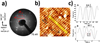 |
Fig. 7 0.7 mL of silicon deposited on NaCl/Ag(110) at 140 °C. (a) LEED pattern showing diffraction spots of Ag, NaCl, and Si in black, blue, and red circles, respectively. (b) STM image (11 × 11 nm2, U = –1 V, I = 1 nA) showing Si chains (yellow rectangle) oriented along the Ag[1-10] direction. (c) Presents the line scans A and B in (b), respectively. |
 |
Fig. 8 0.7 mL of silicon deposited on NaCl/Ag(110) at 140 °C followed by a post-annealing at 200 °C (a) STM image (21.5 × 21.5 nm2, U = –0.7 V, I = 0.8 nA) of a Si ad-layer. (b) High-resolution STM image (5 × 5 nm2, U = –0.04 V, I = 2.6 nA) showing the atomic structure of the deposited silicon self-assembled to form honeycomb-like structure. (c) LEED pattern showing diffraction spots of Ag, NaCl, and Si in black, blue, and red circles, respectively, (d) STM image (7.5 × 7.5 nm2, U = –0.6 V, I = 0.87 nA) of a silicon ad-layer grown on a NaCl film with square symmetry. |
4 Conclusion
We have studied the growth of silicene on NaCl/Ag(110) substrate in the sub-monolayer range using LEED, STM, AES and ARPES experiments. We demonstrate that after covering the metallic surface of Ag with NaCl islands and the deposition of Si atoms by molecular beam epitaxy, the growth of silicene goes through different stages depending on the substrate temperature. Indeed, analysis of the surface after a silicon deposition at room temperature reveals that the Si atoms accumulate on top of the NaCl layer without any long-range order. Furthermore, it was observed that a silicon deposition at 60 °C and 140 °C leads to the formation of an ordered Si chains with a superstructure of (3 × 4). In addition, following a post annealing at 200 °C we have observed that the Si atoms self-assembled to form silicene nanoribbons with a honeycomb-like structure. These results help us understand the growth mechanism of silicene on an insulating substrate and show the importance of the temperature as a factor that can enhance or limit the Si atoms diffusion on the surface, eventually control the growth of silicene [44,45].
Author contribution statement
H. Oughaddou conducted the research project. K. Quertite, H. Enriquez, N. Trcera, A. Bendounan and H. Oughaddou performed the experiments. All authors analyzed the results and contributed to the scientific discussion and the manuscript preparation.
Acknowledgments
This work is supported by a public grant overseen by the French National Research Agency (ANR) as part of the “ Investissements d'Avenir” program (Labex NanoSaclay, reference: ANR-10-LABX-0035).
References
- K.S. Novoselov, A.K. Geim, S. Morozov, D. Jiang, M.I. Katsnelson, I. Grigorieva, S. Dubonos, A.A. Firsov, Nature 438, 197 (2005) [Google Scholar]
- A.K. Geim, K.S. Novoselov, Nat. Mater. 6, 183 (2007) [CrossRef] [PubMed] [Google Scholar]
- M. Derivaz, D. Dentel, R. Stephan, M.C. Hanf, A. Mehdaoui, P. Sonnet, C. Pirri, Nano Lett. 15, 2510 (2015) [CrossRef] [PubMed] [Google Scholar]
- L. Zhang, P. Bampoulis, A.N. Rudenko, Q. Yao, A. Van Houselt, B. Poelsema, M.I. Katsnelson, H.J.W. Zandvliet, Phys. Rev. Lett. 116, 256804 (2016) [CrossRef] [PubMed] [Google Scholar]
- S.Z. Butler, S.M. Hollen, Y.L. Cao, Y. Cui, J.A. Gupta, H.R. Gutiérrez, T.F. Heinz, S.S. Hong, J. Huang, A.F. Ismach, E. Johnston-Halperin, ACS Nano 7, 2898 (2013) [CrossRef] [PubMed] [Google Scholar]
- X. Wu, J. Dai, Y. Zhao, Z. Zhuo, J. Yang, X.C. Zeng, ACS Nano 6, 7443 (2012) [CrossRef] [PubMed] [Google Scholar]
- F.F. Zhu, W.J. Chen, Y. Xu, C.L. Gao, D.D. Guan, C.H. Liu, D. Qian, S.C. Zhang, J.F. Jia, Nat. Mater. 14, 1020 (2015) [CrossRef] [PubMed] [Google Scholar]
- A. Favron, E. Gaufrès, F. Fossard, A.L. Phaneuf-L'Heureux, N. Tang, P.L. Lévesque, A. Loiseau, R. Leonelli, S. Francoeur, R. Martel, Nat. Mater. 14, 826 (2015) [CrossRef] [PubMed] [Google Scholar]
- W. Zhang, H. Enriquez, Y. Tong, A. Bendounan, A. Kara, A.P. Seitsonen, A.J. Mayne, G. Dujardin, H. Oughaddou, Small 14, 1804066 (2018) [CrossRef] [Google Scholar]
- G. Le Lay, B. Aufray, C. Léandri, H. Oughaddou, J.P. Biberian, P. De Padova, M.E. Dávila, B. Ealet, A. Kara, Appl. Surf. Sci. 256, 524 (2009) [CrossRef] [Google Scholar]
- B. Lalmi, H. Oughaddou, H. Enriquez, A. Kara, S. Vizzini, B. Ealet, B. Aufray, Appl. Phys. Lett. 97, 223109 (2010) [CrossRef] [Google Scholar]
- A. Kara, H. Enriquez, A.P. Seitsonen, L.C.L.Y. Voon, S. Vizzini, B. Aufray, H. Oughaddou, Surf. Sci. Rep. 67, 1 (2012) [CrossRef] [Google Scholar]
- S. Cahangirov, M. Topsakal, E. Akturk, H. Şahin, S. Ciraci, Phys. Rev. Lett. 102, 236804 (2009) [CrossRef] [PubMed] [Google Scholar]
- M.R. Tchalala, H. Enriquez, A.J. Mayne, A. Kara, S. Roth, M.G. Silly, A. Bendounan, F. Sirotti, T. Greber, B. Aufray, G. Dujardin, A. Ait Ali, H. Oughaddou, Appl. Phys. Lett. 102, 083107 (2013) [CrossRef] [Google Scholar]
- S. Sadeddine, H. Enriquez, A. Bendounan, P. Das, I. Vobornik, A. Kara, A.J. Mayne, F. Sirotti, G. Dujardin, H. Oughaddou, Sci. Rep. 7, 44400 (2017) [CrossRef] [Google Scholar]
- C.C. Liu, W. Feng, Y. Yao, Phys. Rev. Lett. 107, 076802 (2011) [CrossRef] [PubMed] [Google Scholar]
- P. De Padova, C. Quaresima, B. Olivieri, P. Perfetti, G. Le Lay, Appl. Phys. Lett. 98, 081909 (2011) [CrossRef] [Google Scholar]
- C. Xu, G. Luo, Q. Liu, J. Zheng, Z. Zhang, S. Nagase, Z. Gao, J. Lu, Nanoscale 4, 3111 (2012) [CrossRef] [PubMed] [Google Scholar]
- K. Takeda, K. Shiraishi, Phys. Rev. B 50, 14916 (1994) [CrossRef] [PubMed] [Google Scholar]
- G.G. Guzmán-Verri, L.L.Y. Voon, Phys. Rev. B 76, 075131 (2007) [CrossRef] [Google Scholar]
- L. Meng, Y. Wang, L. Zhang, S. Du, R. Wu, L. Li, Y. Zhang, G. Li, H. Zhou, W.A. Hofer, H.J. Gao, Nano Lett. 13, 685 (2013) [CrossRef] [PubMed] [Google Scholar]
- A. Fleurence, R. Friedlein, T. Ozaki, H. Kawai, Y. Wang, Y. Yamada-Takamura, Phys. Rev. Lett. 108, 245501 (2012) [CrossRef] [PubMed] [Google Scholar]
- H. Oughaddou, H. Enriquez, M.R. Tchalalaa, H. Yildirim, A.J. Mayne, A. Bendounan, G. Dujardin, M. Ait Ali, A. Kara, Prog. Surf. Sci. 90, 46 (2015) [CrossRef] [Google Scholar]
- N.W. Johnson, P. Vogt, A. Resta, P. De Padova, I. Perez, D. Muir, E.Z. Kurmaev, G. Le Lay, A. Moewes, Adv. Funct. Mater. 24, 5253 (2014) [CrossRef] [Google Scholar]
- R. Stephan, M.C. Hanf, P. Sonnet, J. Phys. : Condens. Matter. 27, 015002 (2014) [Google Scholar]
- C.L. Lin, R. Arafune, K. Kawahara, M. Kanno, N. Tsukahara, E. Minamitani, Y. Kim, M. Kawai, N. Takagi, Phys. Rev. Lett. 110, 076801 (2013) [CrossRef] [PubMed] [Google Scholar]
- Y.P. Wang, H.P. Cheng, Phys. Rev. B 87, 245430 (2013) [CrossRef] [Google Scholar]
- J. Repp, G. Meyer, S.M. Stojković, A. Gourdon, C. Joachim, Phys. Rev. Lett. 94, 026803 (2005) [CrossRef] [PubMed] [Google Scholar]
- B. Doppagne, M.C. Chong, E. Lorchat, S. Berciaud, M. Romeo, H. Bulou, A. Boeglin, F. Scheurer, G. Schull, Phys. Rev. Lett. 118, 127401 (2017) [CrossRef] [PubMed] [Google Scholar]
- K. Quertite, H. Enriquez, N. Trcera, Y. Tong, A. Bendounan, A.J. Mayne, G. Dujardin, P. Lagarde, A. El Kenz, A. Benyoussef, Y.J. Dappe, A. Kara, H. Oughaddou, Adv. Funct. Mater. 31, 2007013 (2021) [CrossRef] [Google Scholar]
- K. Quertite, Ph.D. thesis, Silicene growth on insulating ultra-thin film of NaCl, University of Paris-Saclay (ComUE) (2018) [Google Scholar]
- K. Quertite, K. Lasri, H. Enriquez, A.J. Mayne, A. Bendounan, G. Dujardin, N. Trcera, W. Malone, A. El Kenz, A. Benyoussef, A. Kara, H. Oughaddou, J. Phys. Chem. C 121, 20272 (2017) [CrossRef] [Google Scholar]
- K. Quertite, H. Enriquez, N. Trcera, A. Bendounan, A.J. Mayne, G. Dujardin, A. El Kenz, A. Benyoussef, Y.J. Dappe, A. Kara, H. Oughaddou, Nanotechnology 33, 095706 (2021) [Google Scholar]
- L. Mauch, G. Kaindl, A. Bauer, Surf. Sci. 522, 27 (2003) [CrossRef] [Google Scholar]
- W. Hebenstreit, J. Redinger, Z. Horozova, M. Schmid, R. Podloucky, P. Varga, Surf. Sci. 424, L321 (1991) [Google Scholar]
- F.E. Olsson, M. Persson, J. Repp, G. Meyer, Phys. Rev. 71, 075419 (2005) [CrossRef] [Google Scholar]
- S. Heidorn, C. Bertram, J. Koch, K. Boom, F. Matthaei, A. Safiei, J. Henzl, K. Morgenstern, J. Phys. Chem. C 117, 16095 (2013) [CrossRef] [Google Scholar]
- M. Bruno, D. Aquilano, L. Pastero, M. Prencipe, Cryst. Growth Des. 8, 2163 (2008) [CrossRef] [Google Scholar]
- K.D. Childs, Handbook of Auger electron spectroscopy: a book of reference data for identification and interpretation in Auger electron spectroscopy, Physical Electronics, Chanhassen, MN, USA (1995) [Google Scholar]
- M.R. Tchalala, H. Enriquez, A.J. Mayne, A. Kara, G. Dujardin, M.A. Ali, H. Oughaddou, J. Phys. Conf. Ser. 491, 012002 (2014) [CrossRef] [Google Scholar]
- A.Y. Galashev, A.S. Vorob'ev, Phys. Lett. A 408, 127487 (2021) [CrossRef] [Google Scholar]
- L. Tsetseris, S.T. Pantelides, Eur. Phys. J. Appl. Phys. 46, 12511 (2009) [CrossRef] [EDP Sciences] [Google Scholar]
- K. Quertite, H. Zaari, H. Ez-Zahraouy, A. El Kenz, H. Oughadou, A. Benyoussef, Curr. Appl. Phys. 17, 1271 (2017) [CrossRef] [Google Scholar]
- H. Jamgotchian, Y. Colignon, N. Hamzaoui, B. Ealet, J.Y. Hoarau, B.B.J.P. Aufray, J.P. Bibérian, J. Phys.: Condens. Matter. 24, 172001 (2012) [CrossRef] [PubMed] [Google Scholar]
- H. Liu, N. Han, J. Zhao, App. Surf. Sci. 409, 97 (2017) [CrossRef] [Google Scholar]
Cite this article as: Khalid Quertite, Hanna Enriquez, Nicolas Trcera, Pierre Lagarde, Azzedine Bendounan, Andrew J. Mayne, Gérald Dujardin, Abdallah El kenz, Abdelilah Benyoussef, Abdelkader Kara, and Hamid Oughaddou, First steps of silicene growth on an insulating thin-film: effect of the substrate temperature, Eur. Phys. J. Appl. Phys. 98, 41 (2023)
All Figures
|
Fig. 1 LEED diffraction patterns of (a) clean Ag(110) substrate and (b) after 1ML NaCl deposition, recorded at 70 eV and 71 eV electron energies, respectively. The black and blue dashed rectangles show the unit cell of the (1 × 1) and (4 × 1) structures of Ag(110) and NaCl/Ag(110) surfaces, respectively. |
| In the text | |
|
Fig. 2 (a) STM image (800 × 800 nm2, U = –1 V, I = 0.7 nA) of 1ML NaCl on Ag(110) surface (b) atomically resolved STM image of the NaCl layer (3 × 3 nm2, U = –0.2 V, I = 0.7 nA), the NaCl unit cell is indicated by black square line. |
| In the text | |
|
Fig. 3 High resolution ARPES measurements on (a) clean Ag(110) and (b) upon deposition of 1 mL NaCl. The experiments were performed at room temperature at low photon energy of 60 eV. |
| In the text | |
|
Fig. 4 Differential AES spectrum recorded after deposition of 0.5 mL Si on a NaCl/Ag(110) surface. |
| In the text | |
|
Fig. 5 0.2 ML of silicon deposited on NaCl/Ag(110) at room temperature. (a) LEED diffraction pattern showing a (4 × 1) in blue and (2 × 5) in red periodicities assigned to NaCl/Ag(110) surface and silicene/Ag(110) NRs, respectively. (b) STM image (12.5 × 12.5 nm2, U = –1 V, I = 1 nA) showing silicene NRs and a NaCl island (c) STM image (5.5 × 5.5 nm2, U = –1 V, I = 0,8 nA) showing accumulation of Si atoms on the NaCl island. |
| In the text | |
|
Fig. 6 0.2 mL of silicon deposited on NaCl/Ag(110) at 60 °C. (a) LEED pattern showing diffraction spots of Ag, NaCl, and Si in black, blue, and red circles, respectively. (b) STM image (8 × 8 nm2, U = –1.16 V, I = 1 nA) showing an ordered Si structures (yellow rectangle) on a NaCl island with its square symmetry (blue square). |
| In the text | |
|
Fig. 7 0.7 mL of silicon deposited on NaCl/Ag(110) at 140 °C. (a) LEED pattern showing diffraction spots of Ag, NaCl, and Si in black, blue, and red circles, respectively. (b) STM image (11 × 11 nm2, U = –1 V, I = 1 nA) showing Si chains (yellow rectangle) oriented along the Ag[1-10] direction. (c) Presents the line scans A and B in (b), respectively. |
| In the text | |
|
Fig. 8 0.7 mL of silicon deposited on NaCl/Ag(110) at 140 °C followed by a post-annealing at 200 °C (a) STM image (21.5 × 21.5 nm2, U = –0.7 V, I = 0.8 nA) of a Si ad-layer. (b) High-resolution STM image (5 × 5 nm2, U = –0.04 V, I = 2.6 nA) showing the atomic structure of the deposited silicon self-assembled to form honeycomb-like structure. (c) LEED pattern showing diffraction spots of Ag, NaCl, and Si in black, blue, and red circles, respectively, (d) STM image (7.5 × 7.5 nm2, U = –0.6 V, I = 0.87 nA) of a silicon ad-layer grown on a NaCl film with square symmetry. |
| In the text | |
Current usage metrics show cumulative count of Article Views (full-text article views including HTML views, PDF and ePub downloads, according to the available data) and Abstracts Views on Vision4Press platform.
Data correspond to usage on the plateform after 2015. The current usage metrics is available 48-96 hours after online publication and is updated daily on week days.
Initial download of the metrics may take a while.