Fig. 8
Download original image
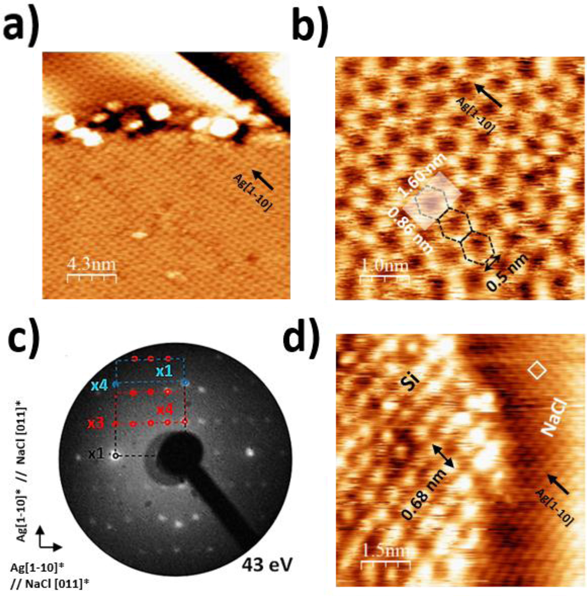
0.7 mL of silicon deposited on NaCl/Ag(110) at 140 °C followed by a post-annealing at 200 °C (a) STM image (21.5 × 21.5 nm2, U = –0.7 V, I = 0.8 nA) of a Si ad-layer. (b) High-resolution STM image (5 × 5 nm2, U = –0.04 V, I = 2.6 nA) showing the atomic structure of the deposited silicon self-assembled to form honeycomb-like structure. (c) LEED pattern showing diffraction spots of Ag, NaCl, and Si in black, blue, and red circles, respectively, (d) STM image (7.5 × 7.5 nm2, U = –0.6 V, I = 0.87 nA) of a silicon ad-layer grown on a NaCl film with square symmetry.
Current usage metrics show cumulative count of Article Views (full-text article views including HTML views, PDF and ePub downloads, according to the available data) and Abstracts Views on Vision4Press platform.
Data correspond to usage on the plateform after 2015. The current usage metrics is available 48-96 hours after online publication and is updated daily on week days.
Initial download of the metrics may take a while.