| Issue |
Eur. Phys. J. Appl. Phys.
Volume 100, 2025
Special Issue on ‘Electromagnetic modeling: from material properties to energy systems (Numelec 2024)’, edited by Lionel Pichon and Junwu Tao
|
|
|---|---|---|
| Article Number | 14 | |
| Number of page(s) | 9 | |
| DOI | https://doi.org/10.1051/epjap/2025010 | |
| Published online | 20 May 2025 | |
https://doi.org/10.1051/epjap/2025010
Original Article
Modeling lightning surface current plates: S-PEEC analytical formulation and experimental validation
1
Safran Tech, Rue des jeunes Bois, 78117 Châteaufort, France
2
ENS Paris Saclay, 4 avenue des sciences, 91190 Gif-sur-Yvette, France
3
GeePs − CentraleSupélec, CNRS, Université Paris-Saclay, Sorbonne Université, 91190 Gif-sur-Yvette, France
4
Safran Electronics and Defense, 86280 Saint-Benoît, France
* e-mail: This email address is being protected from spambots. You need JavaScript enabled to view it.
Received:
18
October
2024
Accepted:
21
March
2025
Published online: 20 May 2025
Abstract
This paper presents an innovative approach based on the partial element equivalent circuit (PEEC) method and the analytical integration of its coupling equations.. Emphasis is placed on the implementation of a surface-based formalism, referred to here as S-PEEC (surface-PEEC). The theoretical principles are explained and confirmed by experimental tests on a planar mock-up. To showcase the versatility of the numerical model, various configurations—including different positions, materials, and calculation domains—are explored. A comprehensive description of the experimental setup is provided, followed by a comparison between the measured current distributions and those obtained through simulations using the S-PEEC formulation, which validates the proposed methodology.
Key words: PEEC method / analytical integration / experimental validation / electromagnetic modeling / lightning
© D. Cvetkovic et al., Published by EDP Sciences, 2025
 This is an Open Access article distributed under the terms of the Creative Commons Attribution License https://creativecommons.org/licenses/by/4.0 which permits unrestricted use, distribution, and reproduction in any medium, provided the original work is properly cited.
1 Introduction
Aircraft lightning strikes are inherently unpredictable and unavoidable, with aircraft typically being struck every 1500 to 5000 flight hours—approximately once a year. According to [1], the phenomenon of lightning involves complex interactions between the aircraft and the surrounding atmospheric conditions, directly affecting the structural integrity of the aircraft and potentially causing significant damage. The effects of lightning on an aircraft can be categorized as direct and indirect. Direct effects include physical damage to the aircraft's structure, such as punctures, burn marks, and possible structural failure. Indirect effects, as highlighted by [2], involve induced currents and electromagnetic interference (EMI), which may compromise the aircraft's electronic systems and overall operational safety. These electromagnetic phenomena require a thorough understanding of electromagnetic compatibility (EMC) to ensure that the aircraft's systems can withstand and operate correctly under lightning-induced disturbances.
Zoning studies identify areas most likely to be struck and their associated potential severity of strikes from a certification perspective [3]. Ensuring aircraft safety and certification involves rigorous testing and adherence to aviation standards such as DO160 [4]. When an aircraft is stroke or attached by lightning, it becomes part of the lightning channel. The strong lightning current flowing through the aircraft and the accompanying time-varying electromagnetic fields interacts with and penetrates the aircraft surface and structure and form the internal electromagnetic environment through various coupling mechanisms [5]. A common configuration in aircraft used to evaluate lightning effects, presented in this paper, is the mock-up consisting of two plates connected by a thin bridge. This setup enables detailed studies of conductive paths and resistance changes during lightning strikes, which are critical for considering the voltage drops due to direct or induced lightning currents passing through the high resistance of composite materials. In practice, aircraft structures like the fuselage or wing surfaces are composed of materials, such as aluminum in older models and, increasingly, carbon fiber composites in newer ones, both of which have distinct electrical properties and lightning strike vulnerabilities. The thin bridge in our experimental setup represents a controlled way to simulate and study the conductive paths and resistance changes that can occur in these materials during lightning attachment. Investigation of electromagnetic effects with this or similar setups that replicate potential current pathways, provides insights to guide the design of lightning protection systems.
Furthermore, an emerging framework involves modeling these effects using numerical methods such as finite-difference time-domain (FDTD), method of moments (MoM), and finite element (FE), as well as combinations thereof. These models help predict and mitigate the effects of lightning strikes on aircraft, providing valuable insights. Among these methods, the partial element equivalent circuit (PEEC) approach is of particular interest. The original PEEC approach, as described in [6–8], involves discretizing a structure into small elements and computing mutual inductance and capacitance through numerical integration over these elements. This process is computationally intensive due to the need for high-dimensional integrals, particularly when dealing with complex geometries. Each element interacts with every other element, leading to dense interaction matrices that scale quadratically with the number of elements. The initialization, storage, and manipulation of these matrices require substantial computational resources and time, making the method highly demanding for large-scale problems.
The work in [9,10] has significantly contributed to the development of the PEEC method, although it presents certain limitations. The conductors must be arranged in either parallel or perpendicular orientations with rectangular cross-sections, and the analytical integrations are restricted to specific configurations, such as coplanar surfaces in 2D and parallelepipeds with parallel faces in 3D. In line with these limitations, [11] introduces an analytical approach aimed at alleviating the computational burden associated with numerical integration. By deriving closed-form solutions for the integrals over non-orthogonal coplanar quadrilaterals, this method significantly reduces the computation time for these interactions. The analytical approach simplifies the integral calculations by transforming them into line integrals, thus avoiding the high computational cost of numerical integration. While the coplanar assumption simplifies the mathematical treatment, but it cannot be easily extended to non-coplanar or more complex three-dimensional geometries, thereby limiting the flexibility of this approach.
The PEEC method, as presented in its analytical formalism by reference [12], shows promise in modeling lightning-induced electromagnetic interactions on aircraft structures. This proposal aims to advance the method towards more complex configurations. Unlike the conventional PEEC formalism, where the integral equations are solved numerically, our approach employs an analytical resolution, offering significant advantages in terms of computation time and computing resources. The innovative aspect concerns the geometry and orientation of the rectangular elements, which are no longer strictly constrained to a parallel or orthogonal arrangement. This paper presents the analytical resolution methodology considering the variable orientation of rectangular elements (see Sect. 2), various time- and frequency-domain PEEC simulations (see Sect. 3), and a comparison between simulated values and experimental measurements (see Sect. 4).
2 Numerical approach
2.1 Theoretical principle
In the conventional PEEC method, the vector potential  is used to calculate inductive coupling between different elements of the discretized structure. The vector potential is a fundamental concept that simplifies the computation of the magnetic field generated by a current distribution. Specifically, in the S-PEEC approach, the expression of the vector potential is used in a surface form. The potential
  created by a surface current density
  at a point M outside the conductor S1, is shown in equation (1).
 (1)
(1)
To facilitate integration, we consider rectangular conductors with current densities  (resp.
  ) running along the axis
  (resp.
  ) as defined in Figure 1.
By substituting equation (1) into the relation defining the partial mutual inductance between two plates [6], we derive expression (2), which generalizes the calculation of the partial inductance between two conductors S1 and S2.
 (2)
(2)
The division of the current density in a conductor along the two axes gives a directional matrix which is dependent on the direction of the evaluated mutual inductance. The length lai with a ∈ {y,z} and i ∈ {1,2} represent the cross section of the conductor as defined in Figure 1.
The second part of the equation involves successive integrations of the distance function. This article presents a methodology offering an analytical calculation of equation (2), with the steps detailed in the following section.
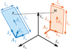 |
Fig. 1 Geometric description of two planar conductors S1 and S2 carrying surface current densities along the z-axis. |
2.2 Methodology
This methodology utilizes a quadrilateral surface mesh, which simplifies the integration process and gives rise to the name S-PEEC (surface PEEC). The x-dimension is disregarded, with integration is performed exclusively over the y and z dimensions. Beginning with the definition of the numerical model of the object under test (OUT), the methodology proposed in this work follows these steps:
1. Meshing the object:
Mesh the OUT to obtain a collection of quadrilateral elementary cells (ECs), which are here two thin plates.
2. Defining the coordinate systems:
Attach local coordinate systems to each conductor, denoted as A1 for conductor 1 and A2 for conductor 2 (see Fig. 1).
Align the axes with the directions of the edges of the elementary cells to form orthogonal reference marks O0.
3. Specifying points:
Define generic points P(y1, z1) on conductor 1 and M(y2, z2) on conductor 2 in their respective local coordinates as shown in Figure 2.
4. Vector projections:
Calculate the positions of points P and M in the global reference frame using vector projections.
5. Calculating distances:
Compute the distance between points P and M using the coordinates:
 (3)
(3)
Here, Δa1, Δa2, with a ∈ {x, y, z} are the distances along each axis in their respective coordinate systems. As described in Figure 2, we obtain
 (4)
(4)
 (5)
(5)
 (6)
(6)
6. Analytical calculation:
Each elementary cell of the mesh is modeled as an equivalent circuit containing four resistances and four inductances, determined by the cell's dimensions (see Fig. 3). To streamline calculations, the mesh is subdivided into four sub-cells, increasing the total number of cells from “N” to “4N”. This subdivision enables the initialization of mutual inductances (M) using a 4N × 4N impedance matrix. The process is automated, with the calculation of inductive couplings and resistances performed over the discretized facets using the PEEC method. This forms an RLM matrix for the output, where the resistance R is directly derived from the cell's dimensions, thickness, and the material's electrical conductivity. The current density is assumed to be uniform across each element (EC).
7. Determining the impedance matrix:
Determine the system impedance matrix from the calculated matrices.
8. Defining sources and solving:
Define voltage and/or current sources.
Perform numerical resolution of the equivalent electrical circuit formed by the ECs in the time domain.
The focus will be on the seventh step, which relies on the previously expressed relations, particularly equation (2) and the relations from (4) to (6). Let us reintroduce the integral part as:
 (7)
(7)
As mentioned earlier, we are tasked with calculating a four-fold integral. The first two integrations are detailed in appendix A and can be reformulated as shown in Equation (8). The integration limits Δa0 (resp. Δal) is the distance along the axis a with a ∈ {y, z} when a1 = 0 (resp. a1 = lai).
 (8)
(8)
The definition of the two coordinate systems, A1 and A2, along with the transition between them, provides the necessary framework to calculate the remaining two integrals (with respect to z2 and y2).
In this approach, the implementation according to the reference frame O0 eliminates the need to introduce an angular definition or perform integrations over angles. Instead, the method relies on vector projections from the local coordinate systems A1 and A2. This technique simplifies the necessary coefficients for integration, making the process more efficient. By avoiding angular integrations and using straightforward vector projections, it streamlines the calculation of inductive couplings, enhancing computational speed.
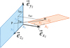 |
Fig. 2 Representation of different points in the coordinate system associated to S1. |
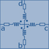 |
Fig. 3 Elementary cell (mesh) and its representation as an equivalent electrical model. |
3 Simulation analysis and model evaluation
3.1 Time and frequency domain simulations
The physical mock-up used for the measurements (see Sect. 4.1) consists of two copper plates, each measuring 200 mm × 300 mm, along with a movable copper link of 45 mm x 30 mm, designed to simulate various conditions.
To comprehensively assess the method's capabilities, the analysis began with frequency-domain evaluations. Lightning strikes are characterized by rapid rise times and high peak currents. A standard representation of lightning current, known as Waveform A, includes components with a broad range of frequencies. In this study, the injected waveform reached frequencies up to 1 MHz and the results of this frequency domain analysis are presented in Figure 4.
This was followed by time-domain simulations using the same numerical setup, enabling us to evaluate the tool's performance in both domains. Notably, the calculation time for the time-domain analysis was reduced compared to the initial frequency-domain simulation, as the RLM matrix had already been determined.
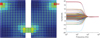 |
Fig. 4 Simulated frequency current distribution map at 1 Hz (left) and current traces for each mesh cell (right). |
3.2 Coplanar geometry modifications
An additional advantage of the method is its flexibility in accommodating various geometries. Users can adjust the geometry and access straightforward simulated data. This characteristic is particularly valuable not only in the aeronautical field for lightning studies but also in other applicable areas, as it enables continuous studies throughout the pre-design process. Different scenarios are treated in this paper: firstly we proposed to modify the location of the connecting part in the middle of the model. Initially positioned at the bottom, as shown in Figure 5, the middle part was moved upwards in two different models: in the first model, it was repositioned slightly higher (12 cm from the top), while in the second model, it was placed at the top (2 cm from the upper edge). The simulations were performed in the time domain.
As shown in Figure 5, the warmer colors indicate the current distribution path, which clearly changes when the middle part is repositioned. The simulated map provides a useful visualization of this distribution. For a better insight, a more refined mesh could be used; in this case, a 2 cm × 2 cm element size was selected to align with the probe dimensions used during experiments (see Sect. 4). However, for more detailed analysis, it is recommended to rely on the calculated current values and traces. Regarding calculation time, it remains consistent with the initial simulation since each modification to the geometry alters the interactions between elements, requiring re-calculation of the RLM matrix.
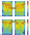 |
Fig. 5 Simulated current distribution map of movable middle part models at peak value. |
3.3 Non-parallel element simulations
The originality of this work lies in the flexibility of analytical S-PEEC solving, and its applicability to non-parallel angle configurations. The following section explores this capability in detail. Specifically, it examines models where second plate is inclined at 30° in the first case and 90° in the second.
As with the previously analyzed models, the surface current distribution is depicted in Figure 6. The following section will closely analyze the factors that distinguish these models from the initial one. As shown in Table 1, the key difference lies in the values of the partial mutual inductance. Notably, when the second plate is inclined by 30°, the inductance values decrease slightly, which can be attributed to the increased distances between the elements. As expected, in the second model, the mutual inductance between orthogonal elements is inherently zero due to the current orientation of the sub-cells. These observations demonstrate the consistency and accuracy of the mutual partial inductance calculations in the S-PEEC approach. Moreover, this behavior is further reflected in the current values in the cells of the second plate, as shown in Table 2. The peak current values decrease for the inclined models, with the 30° inclination showing a moderate reduction and the 90° inclination exhibiting a more pronounced decrease. This report is consistent with the mutual inductance findings, indicating that the geometric orientation of the plates significantly impacts both the inductance and the resulting current distribution.
 |
Fig. 6 Simulated current distribution map of second plate inclination by 30° (left) and by 90° (right). |
Current evaluation in the sub-cells along the x-direction of the second plate for the illustrated models at peak value.
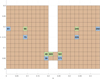 |
Fig. 7 Positions of ECs highlighted for mutual coupling analysis (blue) and current amplitude comparison (green). |
3.4 Material conductivity variations
In order to assess the method's flexibility, the upcoming section explores models that modify material conductivity in designated regions of the model. Modifying the electrical conductivity of specified elementary cells is straightforward. In both scenarios, the conductivity in the specified regions is adjusted to 106 S/m, while the rest of the model remains set to the conductivity of copper 5.96 × 10⁷ S/m. In the first case, the conductivity of the cells within the movable part is modified, while in the second case, the conductivity of the entire second plate is modified, as illustrated in Figure 8.
It is important to note that the following results show the current in the first RL branch along the x-direction of the ECs (see Fig. 3). Figure 9 displays the current amplitude over time circulating through elementary cells (ECs) 40, 303, and 181, which are located near or on the movable part. The data is presented for the initial model, as well as for models with modified conductivity in the movable part and in the second plate. The results indicate that for EC 40, the current amplitude remains significantly lower than that of ECs 303 and 181, regardless of the modifications. This suggests that the position of EC 40 within the model has a noticeable impact on current distribution, as it is positioned on the same plate as the injection.
For ECs 303 and 181, the current amplitude is higher, indicating greater sensitivity to changes in conductivity. Both models #1 and #2 show a reduction in peak current, with slight differences, with a slight modification in the overall shape of the current decay across the models. This suggests that while the material's conductivity influences the magnitude of the current, the time-dependent behavior of the current is affected to a lower degree.
Figure 10 illustrates the current propagation further away from the movable part on both plates. The comparison between the initial model and model #1 shows negligible differences in current behavior. However, in model #2, variations are observed in EC 225, likely due to the changes in material conductivity.
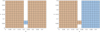 |
Fig. 8 Elementary cell mapping of a planar model, highlighting regions with copper and conductive material of 1e6 S/m (shown in blue). Model #1 (left) represents the modified movable part, while Model #2 (right) depicts the modified second plate. |
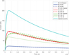 |
Fig. 9 Current amplitude over time for elementary cells (EC) 40, 303 and 181, comparing the initial model with models modified by altering the conductivity. |
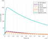 |
Fig. 10 Current amplitude over time for elementary cells (ECs) 95 and 225, comparing the initial model with models modified by altering the conductivity. |
3.5 Simulation time evaluation
Table 3 presents the simulation times for different model configurations, highlighting the computational effort required for each setup. The initial model serves as the baseline, with a total simulation duration of 662.47 s (≈11 minutes) performed on a 13th Gen Intel® Core™ i5-1345U (1.60 GHz). Adjustments to the geometry as shown previously, result in varying simulation times, with the top-positioned middle-part model being the most efficient at 533.33 seconds. Inclining the second plate by 30° and 90° significantly increases the computation time, particularly for the 90° inclination, which has the longest total duration of 941.88 seconds. The circuit computation time for this specific configuration is significantly longer due to the presence of extra zeros regarding the mutual inductance part of the RLM matrices (see for instance Table 1). In particular, an additional 25% of zeros appear when comparing the 90° inclination test case to the initial model (i.e., the planar case in Tab. 1), which affects the computational efficiency of the LTspice solver. Additionally, altering the conductivity in specific regions, such as the middle part or the second plate, further impacts the simulation duration. It is mainly the circuit calculation that varies significantly across models, whereas the RLM matrix calculation remains largely consistent, taking around 300 s for each configuration. These variations in simulation time underscore the complexity introduced by changes in geometry and material properties, emphasizing the importance of efficient computational methods in handling such scenarios.
Simulation times for different model configurations.
4 Numerical results and comparison with experimental results
4.1 Experimental setup
To measure the lightning current components, we utilized custom probes developed by Safran Tech. These handcrafted probes, equipped with an internal coil, are sensitive to surface currents, enabling accurate capture both magnetic field components. While the probes performed well for their intended purpose, their performance was evaluated against a Pearson sensor used for calibration. The transfer function and component measurements were found to be satisfactory.
The measurement process begins with defining the mesh, a crucial step in creating an accurate map of the study area. Once the mapping is established, the probe is positioned at the initial position #{n}. A lightning injection is then performed, allowing the measurement of the injected current (Fig. 11). The lightning current components are captured using an oscilloscope, facilitating detailed analysis. The collected data, which includes the current's vector components and maximum amplitude, is recorded and extracted for further examination. After completing the measurements at the current position, the probe is moved to the next location #{n+1} to repeat the process. Each measurement at a single point on the map takes approximately one minute. Consequently, measuring all 304 points is a time-consuming process. The numerical tool offers significant advantages over experimental measurements, as any modification to the geometry would necessitate repeating the entire measurement process, potentially taking up to 5 hours per model.
This setup enables us to simulate and measure the effects of lightning injection on a conductive surface, validating our modeling methodology with accurate and reliable experimental measurements. The results presented in the next section show an agreement with our expectations, thereby ensuring the validity of our approach.
 |
Fig. 11 View of the proposed “Lightning” experimental setup. |
4.2 Numerical setup and results comparison
Figure 12 illustrates the facetization of the object (meshing step) under test (metallic planar model), with a view of the input (‘in' top right) and output (‘out' top left) of the lightning current propagated on the structure.
Figure 13 shows the Cartesian components of the surface currents measured (in red) and simulated (in blue) using the S-PEEC (Surface-PEEC) calculation code developed by Safran Tech [13]. There is an agreement between the measurements and the S-PEEC simulations. Data are normalized to injected current levels; a WF5, as defined by DO-160 is used [4]. Measurements and simulations are performed in the time domain. The maximum currents, both measured and simulated during the tests, are depicted vectorially in Figure 13 and shown in terms of amplitude in Figure 14.
Figure 14 quantifies the gap between measured data (yaxis and diagonal in red) and simulations (x-axis in blue). The proposal of a margin (light blue zone in Fig. 14) of ±6dB enables us to quantify the agreement of the results obtained: 95% of the simulated data points lie within this margin.
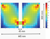 |
Fig. 12 Simulated current map (peak value) and EC mesh. |
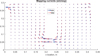 |
Fig. 13 Mapping of normalized currents (at the injection level achieved) including: S-PEEC simulations (blue) and measurements (red). |
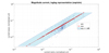 |
Fig. 14 Comparison of measured values (red) VS S-PEEC simulations (blue) of normalized currents. The proposed blue surface delimits a margin of +/− 6dB around the measured values (light blue zone). |
5 Conclusion
In conclusion, this study demonstrates the flexibility and accuracy of the analytical PEEC approach in handling diverse geometries and material properties. We successfully validated the method's capability to simulate planar models and explored its application to more complex scenarios, such as inclined plates and varying material conductivities. The modifications to the geometry and material properties, particularly the use of materials with lower conductivity in different regions of the model, highlight the method's adaptability. Furthermore, the consistency of the mutual partial inductance calculations reinforces the reliability of the approach. Overall, this study confirms the method's potential for a broad range for use in various electromagnetic modeling applications, particularly in fields where flexible simulation tools are essential for pre-design. As a future direction, ongoing research will focus on a comprehensive comparison between analytical and numerical integration, aiming to provide a detailed and quantitative assessment of computational gains.
Funding
The research was funded by Safran and ANRT (Association Nationale de la Recherche et de la Technologie in French) grant number CIFRE 2023/0710.
Conflicts of Interest
The authors have nothing to disclose.
Data availability statement
This article has no associated data generated and/or analyzed.
Author contribution statement
This research was collaboratively developed and reviewed by all authors: Danica Cvetkovic (D.C.), Sébastien Lalléchère (S.L.), Vincent Melchor (V.M.), Lucas Pniak (Lu.P.), Yonathan Corredores (Y.C.), François De Daran (F.D.), Pierre-Étienne Lévy (P-E.L.) and Lionel Pichon (Li.P.). Conceptualization, P-E.L., Li.P., D.C.; Methodology, D.C., F.D.; Software, Y.C., Lu.P. and D.C.; Validation, V.M., D.C.; Formal Analysis, Lu.P. and D.C.; Investigation, V.M.; Data Curation, S.L., D.C.; Writing − original draft, D.C.; Writing − Review & Editing, D.C., Li.P., P-E.L. and S.L.; Visualization, D.C.; Supervision: Li.P., P-E.L., S.L.; Project administration, F.D.
References
- V. Andraud, Experimental implementation and study of the lightning swept-stroke along an aircraft, Ph.D. thesis, Université Paris-Saclay, 2022 [Google Scholar]
- E. Perrin, Study of lightning indirect effects on a composite aircraft by numerical simulation, Ph.D. thesis, Université Limoges, 2010 [Google Scholar]
- A. Fay, A. Bigand, Airbus lightning in service experience vs lightning zoning, in International Conference on Lightning & Static Electricity (2015) [Google Scholar]
- RTCA DO-160, Environmental conditions and test procedures for airborne equipment, Sect. 22 & 23, Radio Technical Commission for Aeronautics, Washington, D.C., 2014 [Google Scholar]
- Y. Fang, Discussion on lightning indirect effects test of DO-160, in 2021 Asia-Pacific International Symposium on Electromagnetic Compatibility (APEMC, 2021), pp. 1–4 [Google Scholar]
- A. Ruehli, Equivalent circuit models for three-dimensional multiconductor system, IEEE Trans. Electromagn. Compat. 22, 216 (1974) [Google Scholar]
- M. Bandinelli, A. Mori, G. Galgani, D. Romano, G. Antonini, A.-L.G. Dieudonné, M. Dunand, A surface PEEC formulation for high-fidelity analysis of the current return networks in composite aircrafts, IEEE Trans. Electromagn. Compat. 57, 1027 (2015) [CrossRef] [Google Scholar]
- G. Antonini, A.E. Ruehli, D. Romano, F. Loreto, The partial element equivalent circuit method: The state of the art, IEEE Trans. Electromagn. Compat. 65, 1695 (2023) [CrossRef] [Google Scholar]
- E. Clavel, Towards wiring design tool: The software InCa, Ph.D. thesis, Institut National Polytechnique de Grenoble, 1996 [Google Scholar]
- J. Roudet, E. Clavel, J.-M. Guichon, J.-L. Schanen, Modélisation PEEC des connexions dans les convertisseurs de puissance, Techniques de l'Ingénieur, 2004 [Google Scholar]
- G. Antonini, A. Orlandi, A. Ruehli, Analytical integration of quasi-static potential integrals on non-orthogonal coplanar quadrilaterals for the PEEC method, IEEE Trans. Electromagn. Compat. 44, 399 (2002) [CrossRef] [Google Scholar]
- L. Pniak, Y. Corredores, P.-E. Lévy, S. Lalléchère, F. de Daran, Formulation analytique du calcul des courants foudre pour des applications aéronautiques, in Colloque international et l'exposition sur la Compatibilité ElectroMagnétique (2023) [Google Scholar]
- Y. Corredores, L. Pniak, P.-E. Lévy, S. Lalléchère, F. de Daran, Determination of lightning induced effects in aeronautic systems by analytical formulation, in Proc. ICOLSE 2022 (Zenodo, 2022) [Google Scholar]
- Y. Corredores, L. Pniak, F. de Daran, P.-E. Lévy, Method for simulating the response of an aeronautical system subjected to at least one electromagnetic event, design method making use of such a simulation and associated device, in International Conference on Lightning & Static Electricity (2024) [Google Scholar]
Cite this article as: Danica Cvetkovic, Sébastien Lalléchère, Vincent Melchor, Lucas Pniak, Yonathan Corredores, François De Daran, Pierre-Etienne Lévy, Lionel Pichon, Modeling lightning surface current plates: S-PEEC analytical formulation and experimental validation, Eur. Phys. J. Appl. Phys. 100, 14 (2025), https://doi.org/10.1051/epjap/2025010
Appendix A Mutual inductance calculation
A.1 Method
The calculation of the vector potential corresponds to the integration of the integral of the distance function over all source points P on surface conductor S₁, i.e. along the z1 and y1 axes.
A.2 First integration
We begin along the y₁-axis; however, the order is not critical since the components are interchangeable in the expression for the vector potential. The first integral is then
 (A.1)
(A.1)
as Δy1 = yM1 − y1 gives dΔy1 = − dy1
The integration is then performed using the following variable substitution
 (A.2)
(A.2)
This substitution leads to the following expressions:
 (A.3)
(A.3)
 (A.4)
(A.4)
Equation (9) can then be rewritten as
 (A.5)
(A.5)
where  and
and  . By expressing the inverse hyperbolic function in logarithmic form leads to
 (A.6)
(A.6)
A.3 Second integration
The second integration is performed along the z1 axis. Taking the previous result into consideration, we first compute the antiderivative and then apply the integration limits. The new term is now:
 (A.7)
(A.7)
Using integration by parts, we can differentiate Iy1 as:
 (A.8)
(A.8)
Equation (15) can then be expressed as:
 (A.9)
(A.9)
The first term of the parenthesis corresponds to equation (9) with the Δz1. The second term can be calculated using two variable substitutions:
 (A.10)
 (A.11)
Using this, we obtain the following expression
 (A.12)
Applying the integration limits we obtain
 (A.13)
where  and
and  .
.
A.4 Following steps
The following integrations can be performed by projecting the distances in the second coordinate system via a change of basis, given by:
 (A.14)
 (A.15)
 (A.16)
The calculation is further detail in the patent [14].
All Tables
Current evaluation in the sub-cells along the x-direction of the second plate for the illustrated models at peak value.
All Figures
|
Fig. 1 Geometric description of two planar conductors S1 and S2 carrying surface current densities along the z-axis. |
| In the text | |
|
Fig. 2 Representation of different points in the coordinate system associated to S1. |
| In the text | |
|
Fig. 3 Elementary cell (mesh) and its representation as an equivalent electrical model. |
| In the text | |
|
Fig. 4 Simulated frequency current distribution map at 1 Hz (left) and current traces for each mesh cell (right). |
| In the text | |
|
Fig. 5 Simulated current distribution map of movable middle part models at peak value. |
| In the text | |
|
Fig. 6 Simulated current distribution map of second plate inclination by 30° (left) and by 90° (right). |
| In the text | |
|
Fig. 7 Positions of ECs highlighted for mutual coupling analysis (blue) and current amplitude comparison (green). |
| In the text | |
|
Fig. 8 Elementary cell mapping of a planar model, highlighting regions with copper and conductive material of 1e6 S/m (shown in blue). Model #1 (left) represents the modified movable part, while Model #2 (right) depicts the modified second plate. |
| In the text | |
|
Fig. 9 Current amplitude over time for elementary cells (EC) 40, 303 and 181, comparing the initial model with models modified by altering the conductivity. |
| In the text | |
|
Fig. 10 Current amplitude over time for elementary cells (ECs) 95 and 225, comparing the initial model with models modified by altering the conductivity. |
| In the text | |
|
Fig. 11 View of the proposed “Lightning” experimental setup. |
| In the text | |
|
Fig. 12 Simulated current map (peak value) and EC mesh. |
| In the text | |
|
Fig. 13 Mapping of normalized currents (at the injection level achieved) including: S-PEEC simulations (blue) and measurements (red). |
| In the text | |
|
Fig. 14 Comparison of measured values (red) VS S-PEEC simulations (blue) of normalized currents. The proposed blue surface delimits a margin of +/− 6dB around the measured values (light blue zone). |
| In the text | |
Current usage metrics show cumulative count of Article Views (full-text article views including HTML views, PDF and ePub downloads, according to the available data) and Abstracts Views on Vision4Press platform.
Data correspond to usage on the plateform after 2015. The current usage metrics is available 48-96 hours after online publication and is updated daily on week days.
Initial download of the metrics may take a while.